Showing posts with label intel. Show all posts

Friday, 21 November 2014

Intel promises 10TB+ SSDs thanks to 3D Vertical NAND flash memory

At present solid-state drives with extreme capacities are very expensive and even the best of them cannot match high-capacity hard disk drives for nearline storage applications. However, thanks to the evolution of NAND flash memory in general, and 3D vertical NAND (3D V-NAND) in particular, the situation may change soon and SSDs with 10TB or higher capacities will become reality.
Intel Corp. revealed at its Investor Meeting 2014 event this week that in the second half of 2015 its joint venture with Micron Technology – Intel Micron Flash Technologies (IMFT) – will start mass production of 3D vertical NAND flash memory chips with up to 256Gb (multi-level cell, 2-bit-per cell) or 384Gb (triple-level cell, 3-bit-per cell) capacity. 3D V-NAND flash memory chips will feature 32-layer vertically stacked cell arrays that are “interconnected” using four billion through silicon vias (TSVs).
The upcoming 3D NAND chips from Intel and Micron will enable solid-state drives with capacities simply not possible today. According to Rob Crooke, senior vice president and general manager of Intel’s non-volatile memory group, the 3D NAND will enable 10TB and larger solid-state storage solutions in the next two years.
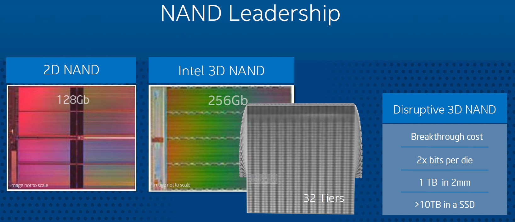
intel 3dnand 3d v nand flash micron 256kb 1024x443 Intel promises 10TB+ SSDs thanks to 3D Vertical NAND flash memory
In a bid to build 4TB Optimus Max solid-state drive earlier this year, SanDisk had to use 64 extremely expensive 64GB (512Gb) eMLC NAND flash memory packages (which integrate four 128Gb eMLC memory chips into one package) that rely on planar NAND flash and are made using thin process technologies. By contrast, Intel’s 256Gb MLC 3D NAND flash memory chip which can hold up to 32GB of data (384Gb/48GB TLC NAND flash) will be made using a mature (i.e., thicker) process technology (Intel does not disclose which one) and will have a “breakthrough” cost. As a result, multi-terabyte solid-state drives will not only become reality, but will not cost several thousands of pounds per unit.
Mr. Crook used a prototype solid-state drive based on the 32-layer 256Gb MLC NAND flash memory to run his presentation at the Investor Meeting 2014, which means that the technology is viable and products on its base are already functional.
At present Samsung Electronics produces 128Gb 24-layer and 32-layer 3D V-NAND MLC NAND memory chips using 42nm process technology. According to Chipworks, “visible” capacity of the 128Gb MLC 3D V-NAND chips is 86Gb, which means that Samsung remains pretty cautious about its multi-layer MLC NAND memory.
Intel’s 3D NAND memory project seems to be far more ambitious than Samsung’s: it will start at 32 layers and 256Gb capacity, which means that Intel’s chips will be more cost-efficient than those from its rival.
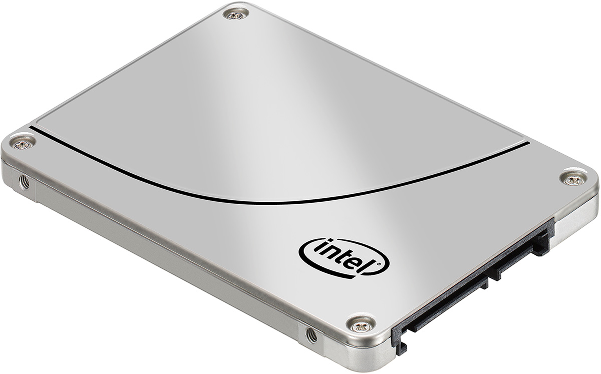
intel ssd enterprise 1 1024x637 Intel promises 10TB+ SSDs thanks to 3D Vertical NAND flash memory
While Intel’s upcoming 3D NAND chips could feature the cheapest cost-per-bit in the industry, its effect on the market of NAND flash-based storage may be limited. IMFT can produce around 70 thousand of 300mm wafers per month, which includes different types of memory, based on data from a ChinaFlashMarket.com report. While Intel and Micron could manufacture their 3D NAND memory at IMFS (80 thousand of 300mm wafers per month) or MTV (40 thousand of 300mm wafers per month) fabs, they will hardly be able to produce volumes comparable to those of Samsung’s. The South Korea-based conglomerate produces 3D V-NAND at its China Xi’an fab that is dedicated to this type of memory and which can process 100 thousand 300mm wafers per month. In addition, Samsung can make 3D V-NAND at other facilities, which total production capacity exceeds 400 thousand 300mm wafers per month.
Although Intel’s 3D NAND may not necessarily revolutionize the market of NAND flash storage in general, it still represents a great opportunity for the company to boost its revenue and SSD market share. Intel NAND and SSD revenue in 2014 is expected to be around $2 billion, thanks to innovations like 256Gb 3D NAND, it will grow further in the coming years.
Source: http://www.kitguru.net/components/memory/anton-shilov/intel-promises-10tb-ssds-thanks-to-3d-v-nand-flash-memory/
If you want to contact RDT please feel free to call between the hours of 9am-8pm AEST. deon@robertsondt.com Ph: 0426279566 or visit https://www.facebook.com/rdtaus

Sunday, 12 October 2014

Lineup of mobile Skylake chips to feature tens of models in 2015

Intel Corp. plans to release a rather broad range of microprocessors based on the Skylake micro-architecture for mobile computers next year, according to a new media report. The upcoming central processing units (CPUs) will address all kinds of mobile devices, including tablets, 2-in-1s, mainstream notebooks as well as high-performance laptops.
As expected, the family of mobile central processing units powered by the Skylake micro-architecture will include three major lines: Skylake-Y for ultra-low-power devices, Skylake-U for mainstream notebooks and Skylake-H for high-end workstation- or gaming-class laptops. Each line will include from four to 15 models, which means that there will be at least 19 different mobile Skylake CPUs net year (four SKL-Y + four SKL-H + 15 SKL-U), reports CPU World.
General specifications of the new chips will look as follows:
  • Skylake-Y (SKL-Y): Core M product line. The chips will feature 2 cores with Hyper-Threading, GT2-class graphics, on-package core-logic set, 3MB or 4MB cache, vPro and TurboBoost technologies. TDP: 4W or lower.
  • Skylake-U (SKL-U): Core i7, Core i5, Core i3, Pentium and Celeron product lines. The chips will feature 2 cores with or without Hyper-Threading, GT1/GT2/GT3/GT3e-class graphics, on-package core-logic set, 2MB, 3MB or 4MB cache, vPro and TurboBoost technologies (on select models). TDP: 15W or 28W.
  • Skylake-H (SKL-H): Core i7, Core i5, Core i3 product lines. The chips will feature 4 cores with Hyper-Threading (Core i3 will feature 2 cores), GT3/GT4-class graphics with or without embedded cache, large L3 caches, vPro and TurboBoost technologies (on select models). TDP: 35W or 45W.
Note: It is unclear which chips support DDR3/DDR3L/LPDDR3 and which also support DDR4.
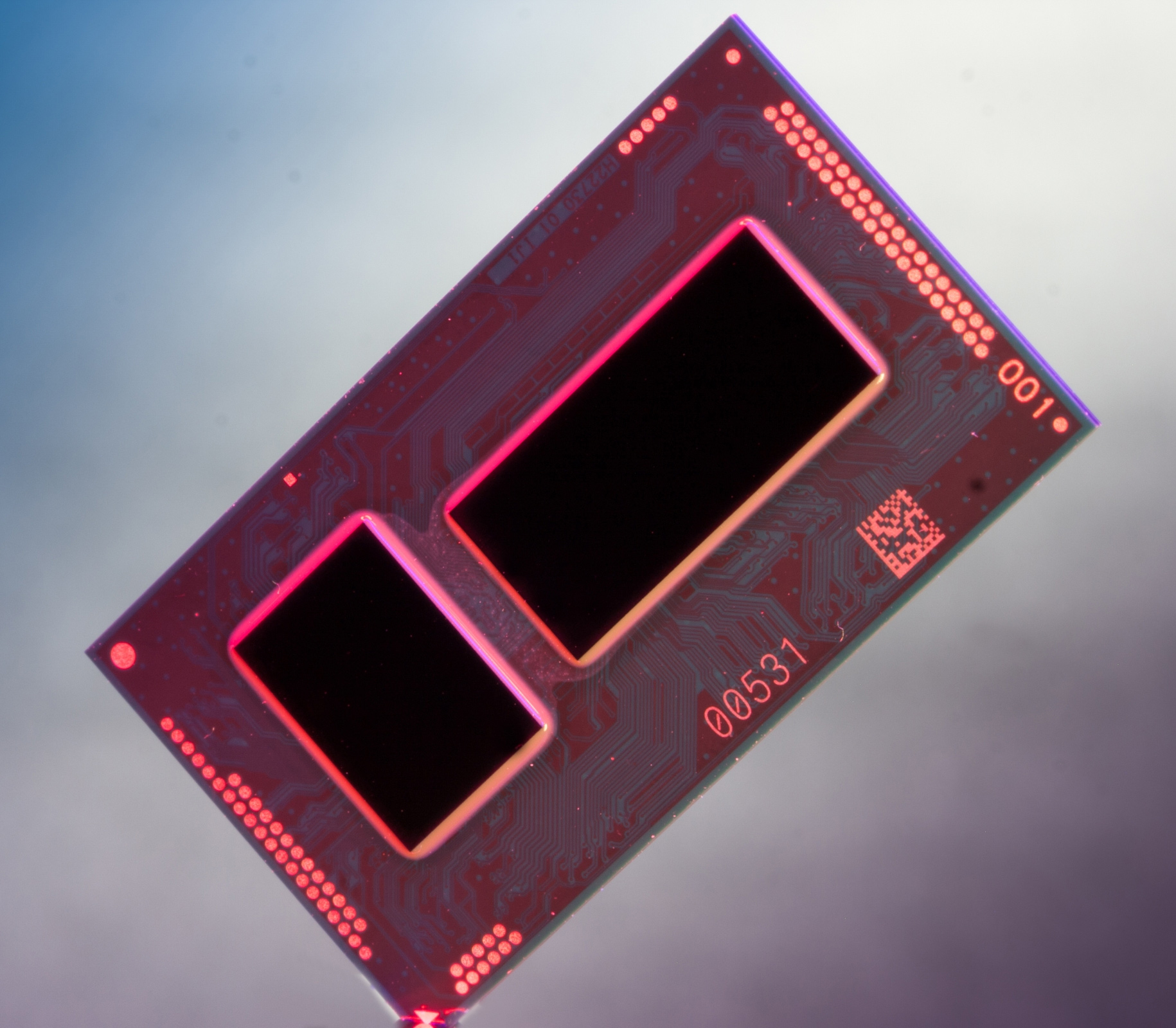
intel core m broadwell 14nm 1024x894 Lineup of mobile Skylake chips to feature tens of models in 2015Intel Core M “Broadwell-Y” processor. Image for illustrative purposes only.
The broad family of mobile Skylake microprocessors indicates that Intel plans to ramp up production of Skylake chips pretty quickly and therefore there will be a lot of systems featuring the latest processors in 2015. Unfortunately, there are no launch details or launch dates for Skylake CPUs.
Central processing units based on Intel’s Skylake micro-architecture are expected to feature considerably improved graphics, a bunch of special-purpose accelerators (e.g., HEVC and VP9 hardware decoders) and support such technologies as AVX 3.2 (512-bit instructions), SHA extensions (SHA-1 and SHA-256, secure hash algorithms), MPX (memory protection extensions), ADX (multi-precision add-carry instruction extensions) and other innovations.
The next-gen Skylake client platform due in 2015 will also be accompanied with numerous connectivity and I/O options, such as Snowfield Peak (Wi-Fi, Bluetooth), Douglas Peak (WiGig, Wi-Fi, Bluetooth), Pine Peak (WiGig), Alpine Ridge (Thunderbolt 3.0 with 40Gb/s transfer rate), Jacksonville Ethernet, next-generation XMM726x-series WWAN 4G/LTE modem and so on. Mobile platforms based on Skylake will support Rezence wireless charging.
Source: http://www.kitguru.net/components/cpu/anton-shilov/lineup-of-mobile-skylake-chips-to-feature-tens-of-models-in-2015/
If you want to contact RDT please feel free to call between the hours of 9am-8pm AEST. deon@robertsondt.com Ph: 0426279566 or visit https://www.facebook.com/rdtaus

Wednesday, 24 September 2014

Eight-core Core i7-5960X overclocked to 6GHz+ with all cores active

Although Intel Corp. decided to set pretty moderate default clock-rate for its eight-core desktop chips aimed at performance enthusiasts, the new Core i7-5960X “Haswell-E” central processing units appear to be pretty good overclockers. Recently a German enthusiast managed to boost clock-rate of the new processor by two times from default using LN2 cooling.
Der8auer, an overclocker from Germany, on Monday overclocked his Core i7-5960X microprocessor from 3.0GHz to 6065MHz, based on his submissions on Hwbot.org, a web-site that overclockers use to share their overclocking results. It is especially noteworthy that all eight cores and the Hyper-Threading technology remained active, as a result, the chip could demonstrate record performance in various applications.
To overclock the eight-core CPU, Der8auer used Gigabyte X99-SOC Force LN2 mainboard based on Intel X99 core-logic set as well as liquid nitrogen (LN2) cooling. The core voltage of the chip was increased to 1.657V, which is not too high.
intel haswell e 6ghz cpuz Eight core Core i7 5960X overclocked to 6GHz+ with all cores active
The record overclocking allowed Deb8auer to set three world’s records for eight-core microprocessors:
  • HWBot Prime – 9698.75 points at 6065MHz;
  • wPrime 1024M – 58.380 seconds at 6065MHz;
  • Cinebench R15 – 2342 points at 5875MHz.
While 6GHz is extremely high clock-rate, it is not the record frequency ever set by the Core i7-5960X chip. Recently Nick Shih, a well-known professional overclocker that works with Asrock, managed to overclock his Intel Core i7-5960X processor to 6594MHz with LN2 cooling on Asrock X99 OC Formula mainboard. He had to increase core voltage to 1.818V and disable seven cores out of eight.
Source: http://www.kitguru.net/components/cpu/anton-shilov/eight-core-core-i7-5960x-overclocked-to-6ghz-with-all-cores-active/
If you want to contact RDT please feel free to call between the hours of 9am-8pm AEST. deon@robertsondt.com Ph: 0426279566 or visit https://www.facebook.com/rdtaus

Monday, 15 September 2014

Intel Skylake Could Feature Dual DDR3/DDR4 Memory Support with Double IMCs

[Not Confirmed] An interesting point raised by the Italian publication Bitsandchips.it, stated that Intel has tucked away a very big hint pertaining to memory support in its IDF14 slide deck. Upon closer inspection the hint is about DDR3 and DDR4 support at the same time probably utilizing a Dual-IMC design . The market is now moving toward DDR4 but its prices remain quite high, so it might be possible that Intel will introduce the above-mentioned tech to hasten the transition.Intel Broadwell and Skylake Platform

Dual-IMC with DDR3 and DDR4 Support Could Grace Skylake Processors – Hints IDF14 Slides

As we told you a long time ago and as Intel later confirmed in IDF14, Skylake-S is coming in 2H 2015, most probably July. These will be quad cores and will come in i5 and i7 variants with 4 and 8 threads respectively. Skylake will of course also arrive on mobile platforms and 2-in 1 devices before the desktop release. If you notice the slide deck below, specifically the one on the right, you will notice that Intel mentions “DDR3 and DDR4″ in the “future” section of the Mainstream segment. Now Intel has noted down Haswell Micro-architecture, so its near future is Broadwell and Skylake-S.
So what does ‘DDR3 and DDR4′ support for the future generations of Intel Haswell mean? Well, one option could be offering some SKUs with DDR3 and other with DDR4, but that would be awfully inconvenient from a marketing and practical point of view. Not only would that discourage growth (DDR3 users will simply buy the DDR3 variant and stick with it) but that will result in disparity between similar products: not an ideal scenario.No, a far easier option would be to introduce dual memory support using a Double IMC (Integrated Memory Circuit) on the processors. A question that comes to mind is whether Broadwell-k will benefit from Double-IMCs as well, or will the rift between the high end and mainstream will grow ever larger.
Intel believes that the pricing of DDR4 will remain high; as will the demand of Skylake processors. Migration to DDR4 should be encouraged but you can’t leave the majority of your user base behind. The answer to this dilemma lies in the company introducing Skylake with both DDR3 and DDR4 support. Intel will favor the use of DDR4 memory but if this is correct than users will not need to be worry about buying new RAMs and instead be able to focus on the new micro-architecture and step up when they are ready. DDR4 not only offers faster RAM memory  with double the density but also offers a greatly lowered electrical foot print with reduced power requirements. DDR4 RAM can be clocked upto 3200Mhz and requires 1.2V of juice to run. CAS latency will vary from 9 to 24 (DDR3 wad 5-14) while density increases from 4GB at 8 banks to 8GB at 16 banks.


Source: http://wccftech.com/intel-skylake-dual-ddr3-ddr4-memory/#ixzz3DNb4ommz


If you want to contact RDT please feel free to call between the hours of 9am-8pm AEST. deon@robertsondt.com Ph: 0426279566 or visit https://www.facebook.com/rdtaus

Thursday, 11 September 2014

Intel Confirms Full Hardware-Level DirectX12 On Skylake-S iGPU

A few days ago I wrote about a leak which stated that Skylake-S will have DX12 support. However, we were not sure whether it was just DX12 API that was supported or the full hardware level feature set. As it turns out, it is the latter as Intel has officially confirmed the same in its IDF 14 keynote. This would also make the upcoming Intel processors the first chips to have confirmed full DX12 support.Intel Broadwell and Skylake Platform

DirectX 12 Hardware-Level Feature Set Will be Supported by Intel Skylake Processors

DX12 needs no introduction, thanks to social media and online publications it is one of the most eagerly anticipated APIs after Mantle. However, even though we have seen demos, tech charts and more, we have yet to see a hardware chip that supports the ‘Feature Level 12_0′ set. Many thought that the upcoming GPUs from Nvidia and Maxwell would be the first to do so, but we still have a few days to go before release and Intel has already swooped in and taken this particular honor.
Intel_Skylake_1st_DX12_FL12_0_hardware-pcgh (1)Slide courtesy of PCGamesHardware.de
Intel’s Skylake-S processors are one of the first confirmed  chips to support the full and uncut DirectX 12. I am 90% sure that Nvidia Maxwell will support the full feature set too, but until its confirmed, it doesn’t count. You will ofcourse be seeing the DirectX12 tag on a lot of devices  but that only indicates support for DX12 API. The actual Direct3D Feature Level 12_0 is what we are after. GPUs/Devices which do not have hardware-level support of DX12 will have Feature Level 11_0, Feature Level 11_1 and Feature Level 11_2 at most. If you take a look at the slide shared by Intel on IDF14 above you will notice that Intel mentions “Next Generation Intel Core Processors” which means Skylake and beyond. It also mentions “Next Gen 14nm Intel Processor for tablets.
Which is something we have suspected for quite some time now. Recall the DX12 demo at SIGGRAPH that showed a massive 60% boost for mobile devices. Since a Mobile Platform is always working with power and thermal constraints, both the CPU and GPU share a TDP Budget if you may, so any lack of power consumption by one can either be utilized in a zero sum or result in a decreased TDP rate. This makes a low level API of critical import to the mobile sector. Most importantly however, this was a very big hint to the press that Microsoft is going to be shaping DX12 for the tablet sector as well. There wasn’t a lot of technical information in this update, but it does tell us that Microsoft seems to have learned from the debacle that was DX10 and is trying to push DX12 non-exclusively into everything and anything it can manage. The OS however, is another story altogether and I won’t be surprised if DX12 is Win 9 only.


Source: http://wccftech.com/intel-confirms-full-hardwarelevel-directx12-skylakes-igpu/#ixzz3D3Kn4zvu


If you want to contact RDT please feel free to call between the hours of 9am-8pm AEST. deon@robertsondt.com Ph: 0426279566 or visit https://www.facebook.com/rdtaus

ASUS Launches Z10PE-D8 WS Dual Socket Motherbaord

ASUS releases its Z10PE-D8 WS motherboard which is based on the Intel C612 chipset. it has dual processor sockets ready for the latest Intel Xeon processor E5-2600 v3 product families. And that means a whole lotta cores.
The new Server System Infrastructure Enterprise Electronics Bay (SSI EEB) motherboards have superb storage support, including the ASUS PIKE II (Proprietary I/O Kit Expansion) card and support for PCI Express (PCIe) 3.0 x4 M.2 (Next-Generation Form Factor, or NGFF). They benefit also from the ASUS Q-Code Logger for one-touch easy maintenance and a Dr. Power LED lamp to clearly indicate unusual power status.
Ultimate PCI Express 3.0 multi-GPU power
The Z10PE-D8 WS is equipped to provide the ultimate workstation graphics power, with support for up to four dual-slot graphics cards. Both 4-Way NVIDIA GeForce SLI and AMD CrossFireX are supported, so it is an excellent choice for professionals who depend on powerful graphics in areas such as design, modeling and medical research, as well as processing-intensive simulation and rendering applications.

With a total of seven PCIe 3.0 slots, the Z10PE-D8 WS offers ample room for RAID cards, PCI Express-based solid-state drives (SSDs), video-capture cards and other high-speed components.

Premium components for premium power efficiency
Z10PE-D8 WS benefits from premium components hand-chosen and carefully arranged by ASUS engineers to provide optimum power efficiency. These include integrated Driver-MOSFETs (Dr. MOS) to save space and reduce operating temperatures for more efficient operation, and ASUS-exclusive Beat Thermal Chokes II. The new Beat Thermal Chokes II design delivers up to 94% power efficiency and lower temperatures under normal operation.

ASUS is the world's first server manufacturer to introduce 12K solid capacitors - the Z10PE-D8 WS has these ultra-resilient components on board. These Japanese-made capacitors are able to withstand up to 12,000 hours of temperatures as high as 105°C, far exceeding everyday demands. And at a typical operating temperature of 65°C, our 12K capacitors have an expected lifespan of 1.2m hours - or well over a century.

The Z10PE-D8 WS also employs ProCool power connectors. The ProCool design eliminates hollow areas associated with traditional power connectors, ensuring a close and secure connection with the PSU power connector pins. The flush connection enables lower impedance and better heat dissipation - helping to prevent connector burnouts.

Flexible fan speed control, flexible storage and easy maintenance
The new Z10PE-D8 WS motherboard offers flexible fan-speed controls, which can be managed manually or automatically. In automatic mode, the fan speeds are adjusted according to the processor temperature. In manual mode, the administrator can set a fan curve according to cooling requirements.

The new Z10PE-D8 WS motherboard offers industry-leading storage flexibility, with a built-in M.2 connector supporting PCIe 3.0 x4 2260 (60mm), 2280 (80mm) and 22110 (110mm) devices, and support for the ASUS PIKE II (Proprietary I/O Kit Expansion) card for high-reliability, enterprise-grade 12Gbit/s Serial Attached SCSI (SAS) devices.

The motherboard also benefits from ASUS Q-Code Logger, an easy-maintenance button that records four-digit port 80 code logs to a flash drive with one touch, so administrators can diagnose problems quickly and easily. Similarly, the conveniently-located Dr. Power LED displays messages to clearly indicate a power fault.

AVAILABILITY & PRICING
The Z10PE-D8 WS is priced at $599 and will be available soon at ASUS authorized resellers and distributors.


If you want to contact RDT please feel free to call between the hours of 9am-8pm AEST. deon@robertsondt.com Ph: 0426279566 or visit https://www.facebook.com/rdtaus

Wednesday, 10 September 2014

Intel unveils new-generation Xeon E5 v3 chips with up to 18 cores

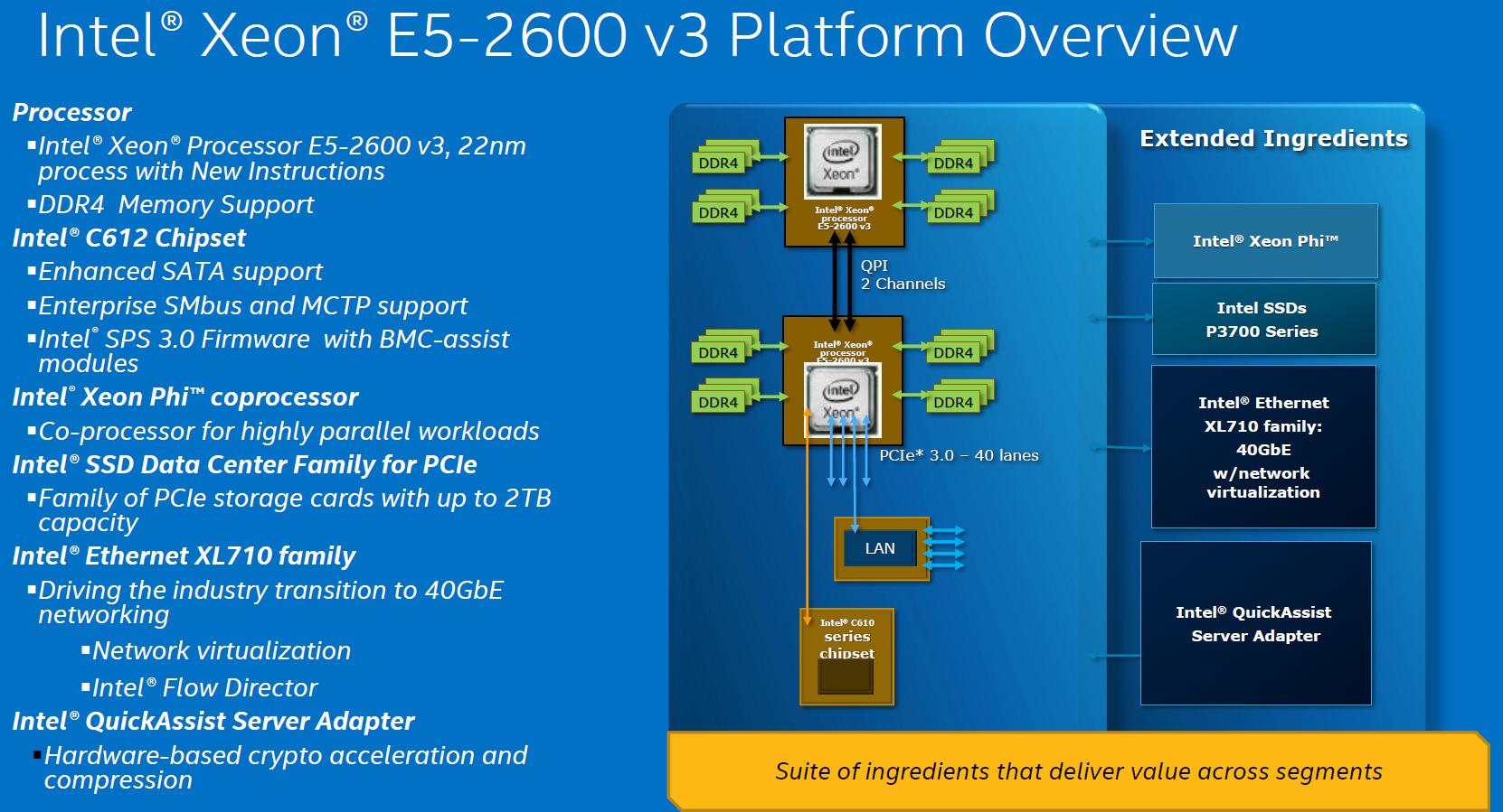
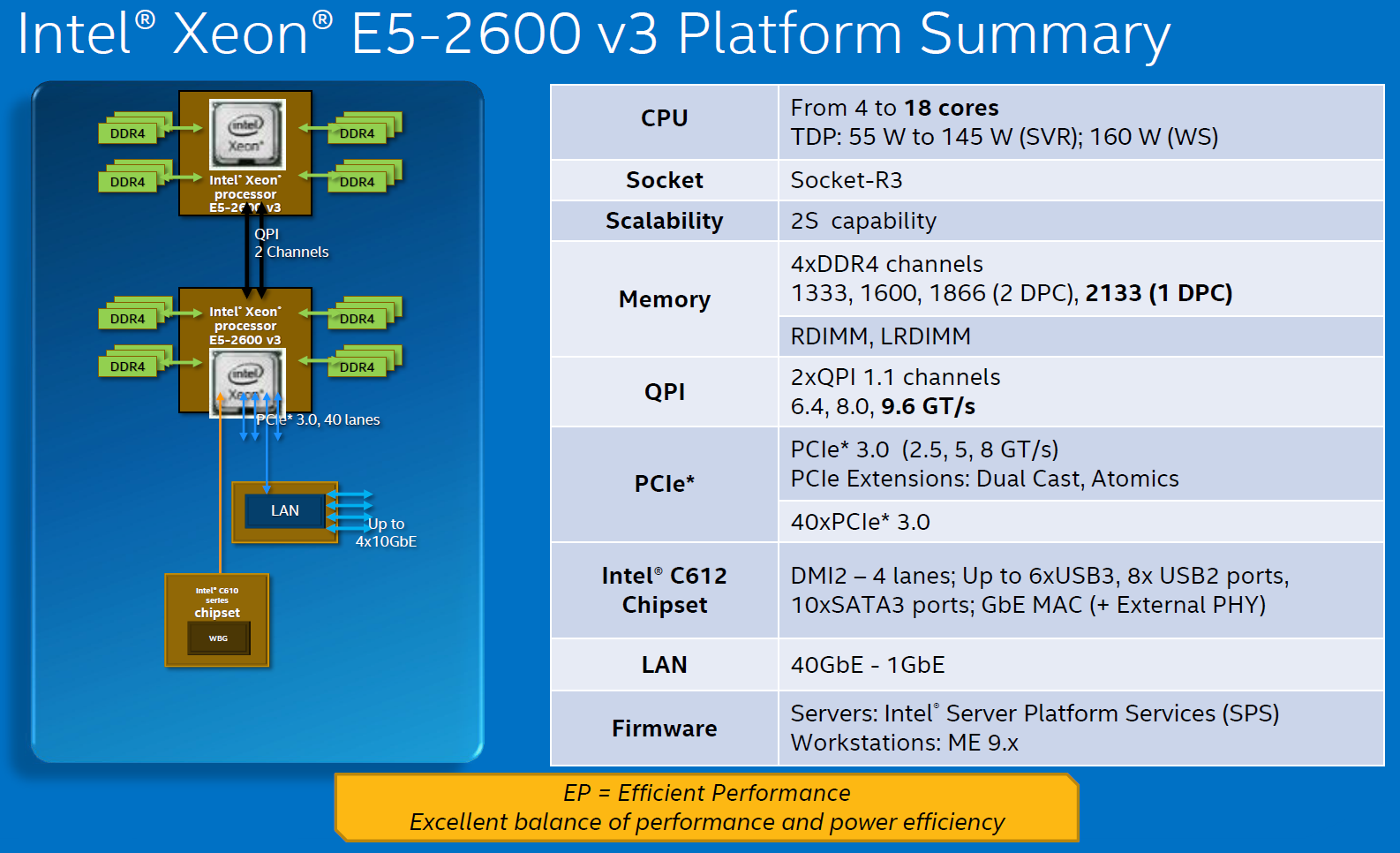
Intel Corp. on Monday rolled-out its new Xeon E5 2600/1600 v3 server processors based on the code-named “Haswell” micro-architecture. The latest server central processing units feature up to 18 cores per chip and quad-channel DDR4 memory controllers, whereas the new C612 platform code-named “Grantley” features a number of innovations that will be available on the market of 2-way servers for the first time.
Intel’s new server platform is not only powered by all-new processors that deliver up to three times higher performance than predecessors (in select cases), but a number of extended ingredients designed to improve security (with the help of QuickAssist server adapter, which provides hardware-based crypto acceleration and compression), speed up network speeds ( thanks to Intel Ethernet XL710 40GbE adapter with network virtualization), reduce power consumption while boosting performance (thanks to DDR4 memory and Intel P3700-series solid-state drives) and improve other server metrics, such as resilience and optimized total cost of ownership. The new processors and platforms will be used in servers, workstations, storage and networking infrastructure to power a broad set of workloads such as data analytics, high-performance computing, telecommunications and cloud-based services, as well as back-end processing for the Internet of Things.
intel xeon e5 v3 haswell overview 1024x553 Intel unveils new generation Xeon E5 v3 chips with up to 18 cores
“The digital services economy imposes new requirements on the data center, requirements for automated, dynamic and scalable service delivery,” said Diane Bryant, senior vice president and general manager of the Data Center Group at Intel. “Our new Intel processors deliver unmatched performance, energy efficiency and security, as well as provide visibility into the hardware resources required to enable software defined infrastructure. By enabling the re-architecture of the data center, Intel is helping companies fully exploit the benefits of cloud-based services.”
intel xeon e5 v3 haswell overview 1 1024x623 Intel unveils new generation Xeon E5 v3 chips with up to 18 cores
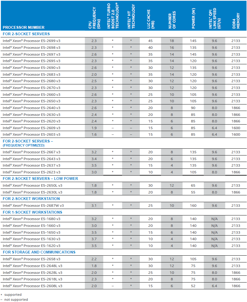
Intel’s new Xeon E5 2600/1600 v3 processors feature 4-18 cores (with or without the Hyper-Threading technology), up to 45MB of L3 cache and 55W – 160W thermal design power. The new chips feature Advanced Vector Extensions 2 (Intel AVX2) extensions that double the width of vector integer instructions to 256 bits per clock cycle for integer sensitive workloads and delivers up to 1.9 times higher performance gains. The new chips also feature Advanced Encryption Standard New Instructions (Intel AES-NI) technology that accelerates data encryption and decryption by up to times without sacrificing application response times.
The Intel Xeon processor E5-2600 v3 product family will be offered with 26 different parts that range in price from $213 to $2702 in quantities of 1000. Intel Xeon processor E5-1600 v3 workstations will be offered with six different parts in prices ranging from $295 to $1723.
Intel’s partners are ready to start shipments of 65 servers based on the new Xeon E5 v3 processors, in the coming months over 77 new systems will become available. In general, there are 250 machines powered by the latest Xeon E5 v3 chips in development.
intel xeon e5 v3 haswell specs Intel unveils new generation Xeon E5 v3 chips with up to 18 cores
If you want to contact RDT please feel free to call between the hours of 9am-8pm AEST. deon@robertsondt.com Ph: 0426279566 or visit https://www.facebook.com/rdtaus

Sunday, 31 August 2014

ASUS Proprietary but Impressive OC Socket Examined – Is it even LGA 2011?

[Mini-Editorial] I was pretty impressed by ASUS’s recent innovation in the socket sector. I am talking ofcourse about the ASUS OC Socket, which boasts improved OC performance by granting the user more stability and higher voltage control thanks to more pins. Now while this all an impressive feat for an AIB to do, it begs the question whether we are looking at LGA 2011 at all.
asus_logo02

Is the ASUS OC Socket Intel LGA 2011 at all? Or is it actually the ‘LGA 2017′ Homegrown Socket?

The LGA 2011-3 is Intel’s Socket designed to be used with its HEDT Processors. Now the 2011 indicates the amounts of pins in the socket and the ’3′ indicates the revision of the socket. Now that means that any LGA 2011 socket will have exactly 2011 pins. So is the ASUS OC Socket LGA 2011 then? Umm, no technically it is not. The ASUS OC Socket is compatible with the LGA 2011 but it is not in reality 2011. If you were to give it a name in Intel’s current nomenclature it would be LGA 2017 (the OC Socket has 6 additional pins apparently). Since ASUS has basically designed a completely new socket, I wouldn’t expect it to be rock solid and completely bug free at launch.
asus_01Let’s take a closer look at what exactly ASUS has accomplished. Haswell uses an FIVR (Fully Integrated Voltage Regulator) and as the new processor architectures have appeared, Intel has become more and more secretive about the workings of the pinouts. Not knowing where the voltage lines lay, ASUS basically bruteforced the entire contact points present on 2011 processors to figure out where the new pins should touch to grant unhindered access to voltage. The result? ASUS OC Socket lets you effectively bypass any FIVR compulsions Intel has in place. This means that you will be able to achieve higher and more stable overclocks probably at a lower voltage. I have a feeling ASUS might be a trend setter with this and seeing they already have a patent pending, might earn big bucks from it too.
And that’s not it either. We already know that Intel is dropping the FIVR, so it doesn’t come as a surprise that it is not that fine tuned because the extra pin outs on an ASUS Proprietary OC Socket allow access to voltage lines for DDR4 Voltage, enabling greater overclocking than you would normally be able to achieve. Now we didn’t receive an ASUS X99 Deluxe engineering sample so Overclockers.ru was kind enough to send us an image of the box art. They claim a 60% improvement in the CPU sector and 12.5% improvement (3000Mhz) for DDR4 RAM. Now there’s something else I noticed here, ASUS’s language is quite loose, these extra six pinouts might just be the six sections where the excess contacts are. Which means that there could be more or less than just six pins. Either way, you know the drill. Whatever the additional pin count is, add that to 2011 and you get the real name of the socket present in these special ASUS mobos.


Source: http://wccftech.com/asus-oc-socket-examined-lga-2011/#ixzz3C0poTe7b


If you want to contact RDT please feel free to call between the hours of 9am-8pm AEST. deon@robertsondt.com Ph: 0426279566 or visit https://www.facebook.com/rdtaus

Thursday, 28 August 2014

Intel i7 5960X, 5930K and 5820K Price

Price: $1199 AU

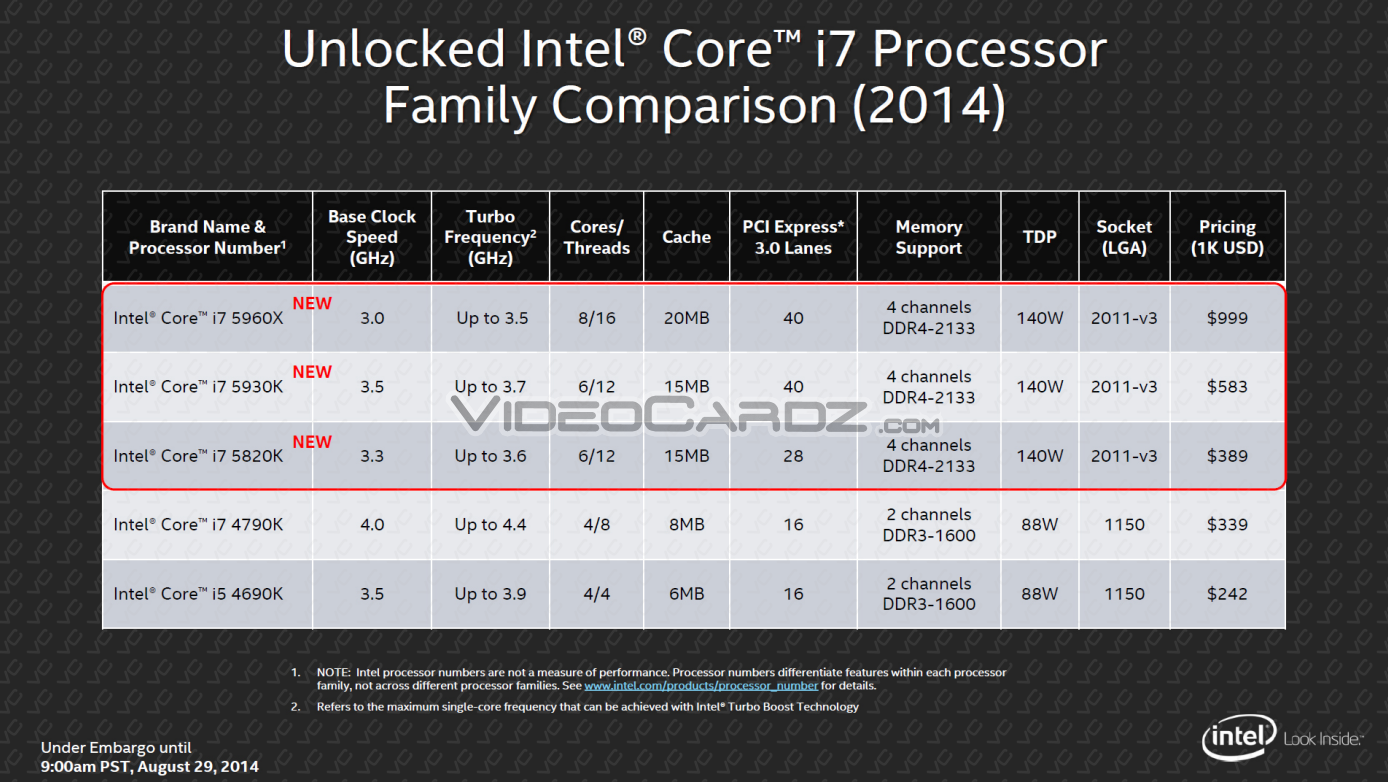
Intel Core i7 5960X Extreme Edition Haswell-E 3.0GHz (3.5GHz Turbo), LGA 2011-3, 20MB Cache, 140W Eight Core with Hyper-Threading. Boxed processor only, CPU cooler is not included.

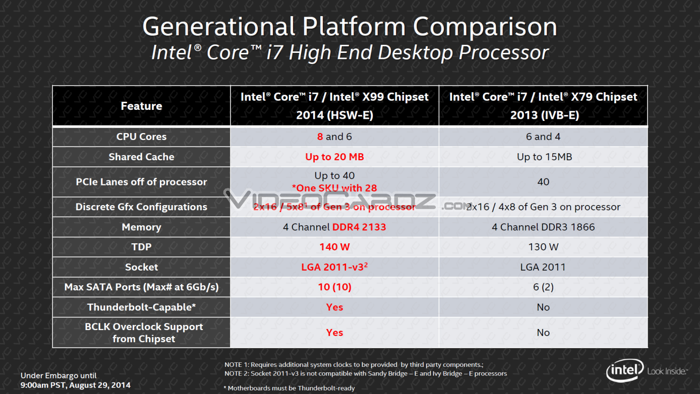
Please note that this CPU is only compatible with LGA 2011-3 motherboards. LGA 2011-3 CPUs are not compatible with LGA 2011 motherboards.


Price: $679 AU

Intel Core i7 5930K Haswell-E 3.5GHz (3.7GHz Turbo), LGA 2011-3, 15MB Cache, 140W Six Core with Hyper-Threading. Boxed processor only, CPU cooler is not included.

Please note that this CPU is only compatible with LGA 2011-3 motherboards. LGA 2011-3 CPUs are not compatible with LGA 2011 motherboards.


Price: $449 AU

Intel Core i7 5820K Haswell-E 3.3GHz (3.6GHz Turbo), LGA 2011-3, 15MB Cache, 140W Six Core with Hyper-Threading. Boxed processor only, CPU cooler is not included.

Please note that this CPU is only compatible with LGA 2011-3 motherboards. LGA 2011-3 CPUs are not compatible with LGA 2011 motherboards.


If you want to contact RDT please feel free to call between the hours of 9am-8pm AEST. deon@robertsondt.com Ph: 0426279566 or visit https://www.facebook.com/rdtaus

Intel Core i7-5960X “Haswell-E” HEDT Flagship Processor Benchmarked and Overclocked To 4.0 GHz

The first benchmarks of Intel’s next generation Core i7-5960X “Haswell-E” processor have been unveiled by Coolaler forums. While several tech sites including us have the X99 and Haswell-E review planned for 29th August, Coolaler went ahead to showcase a performance preview of the upcoming Core i7-5960X processor which is the flagship SKU of the Haswell-E lineup.
Intel Haswell-E Core i7-5960X

Intel Core i7-5960X “Haswell-E” HEDT Flagship Processor Benchmarked

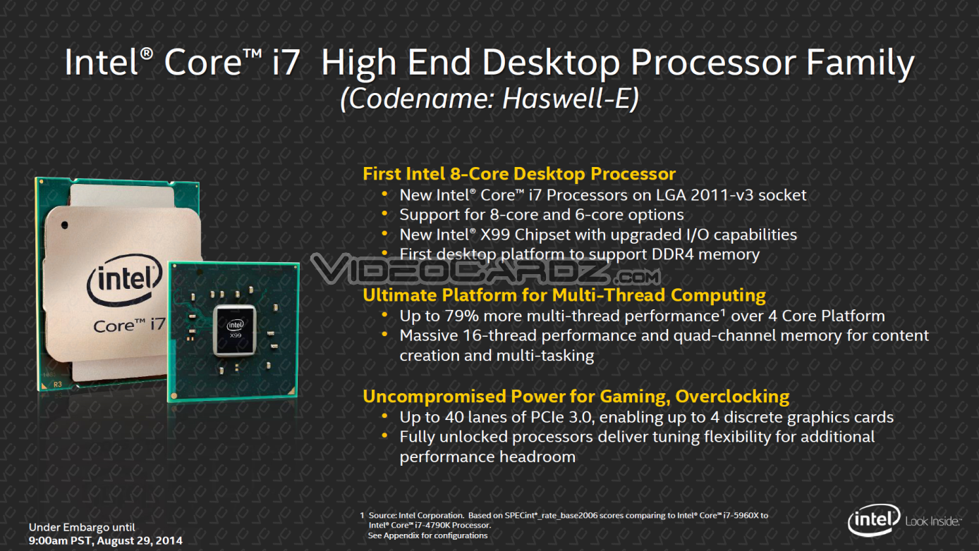
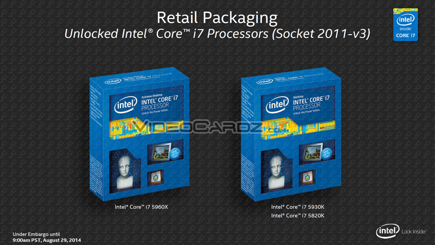
We have most of the details regarding the Haswell-E processors thanks to the leak from Videocardz earlier this week. The Intel Haswell-E processor lineup would include three SKUs, the Core i7-5960X, Core i7-5930K and Core i7-5820K. All processors are built on the 22nm Haswell architecture which means that they will improve the IPC performance while keeping the same power limits as previous generation processors due to enhanced power efficiency of the Haswell microarchitecture. Before moving into the feature set of the platform itself, we will detail the SKUs that will be launching in 29th August 2014:

Intel Core i7-5960X Processor


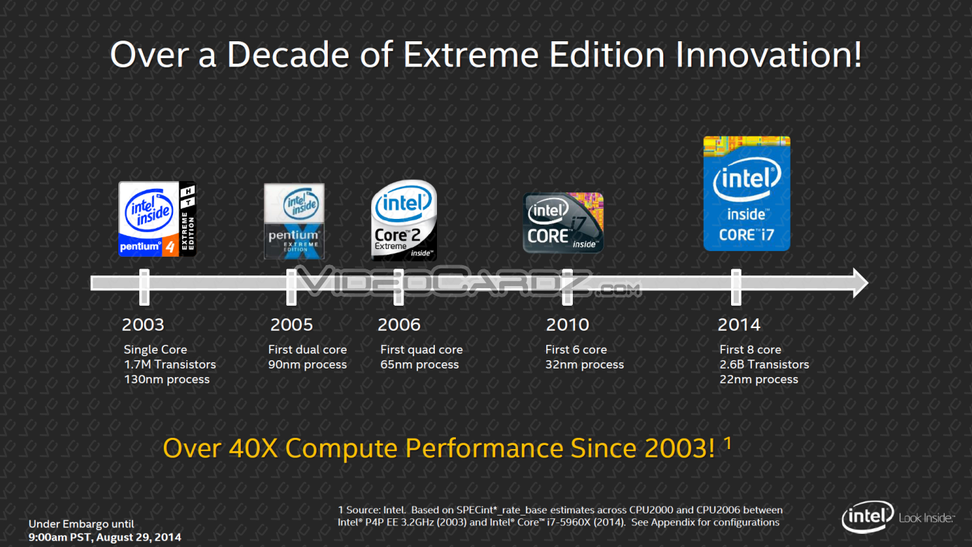
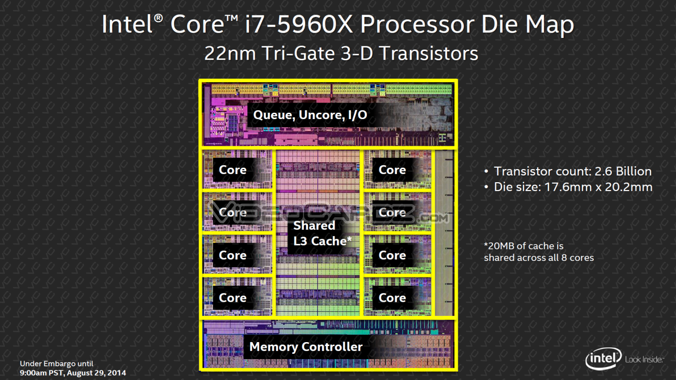
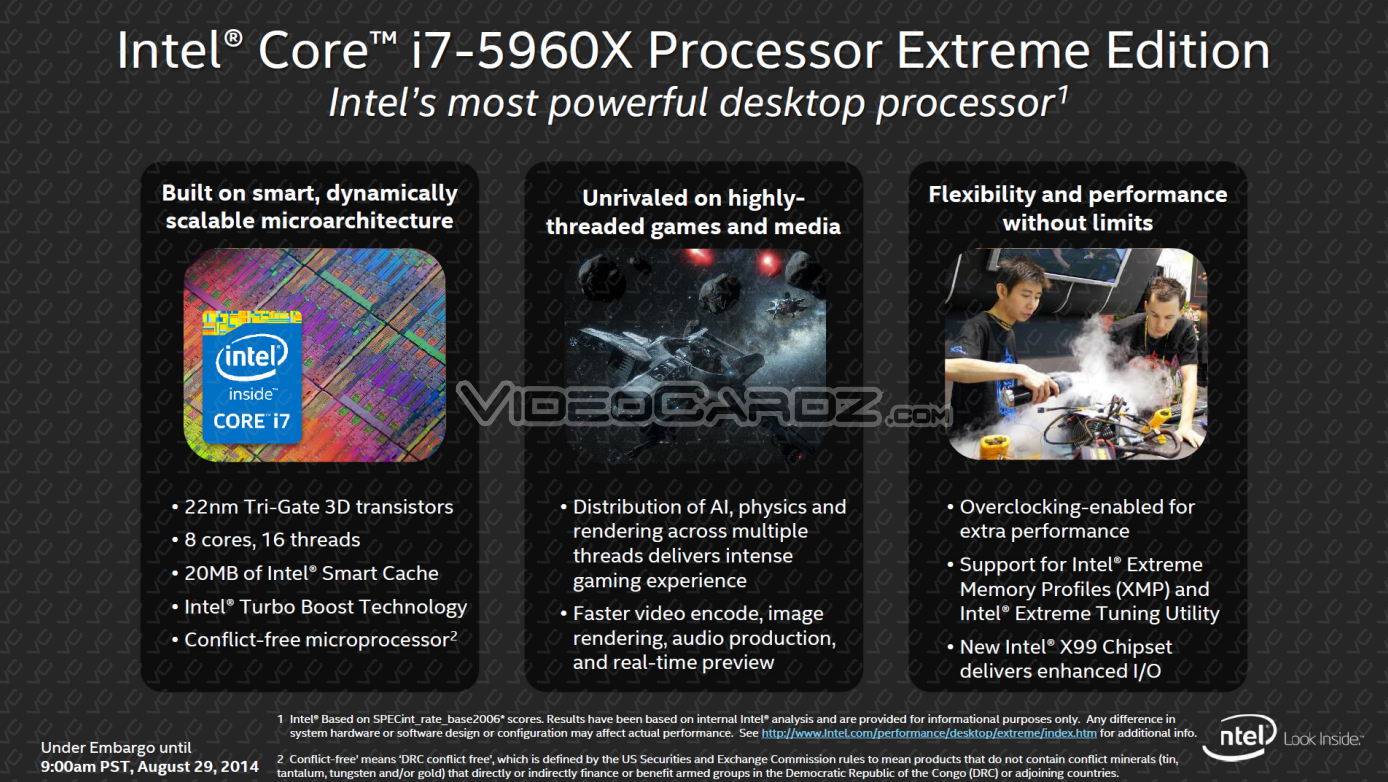
The Intel Core i7-5960X Extreme Edition would be the flagship processor of the lineup boasting 8 Cores and 16 threads. The Haswell-E Core i7-5960X will house 2.6 Billion transistors inside its 22nm die and measures at 335.2 mm which is considered a huge die. The die block diagram also shows that the Core i7-5960X is not a 12 core die as previously expected which turns out to be a Xeon core. We can see 8 Cores with a large amount of shared L3 cache in the middle with a DDR4 memory controller at the bottom and Queue, Uncore and I/O at the top side. This would be Intel’s first 8 Core consumer processor and would be clocked at 3.0 GHz base and 3.5 GHz boost frequency. The processor would feature 20 MB of L3 cache, 140W TDP and support for DDR4-2133 MHz memory. Being the flagship processor of the Haswell-E lineup, the Core i7-5960X would end up with a price of $999 US.
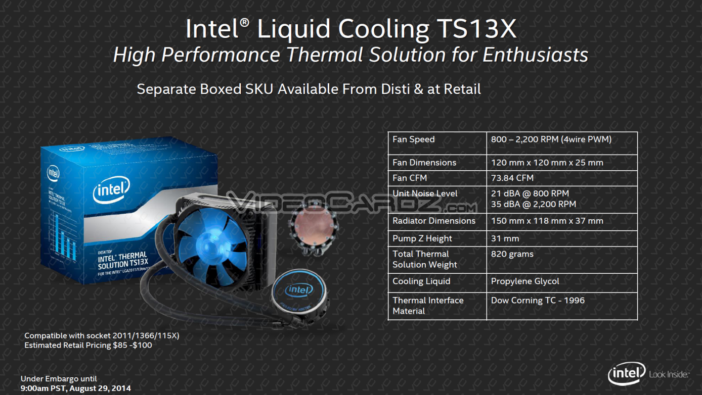
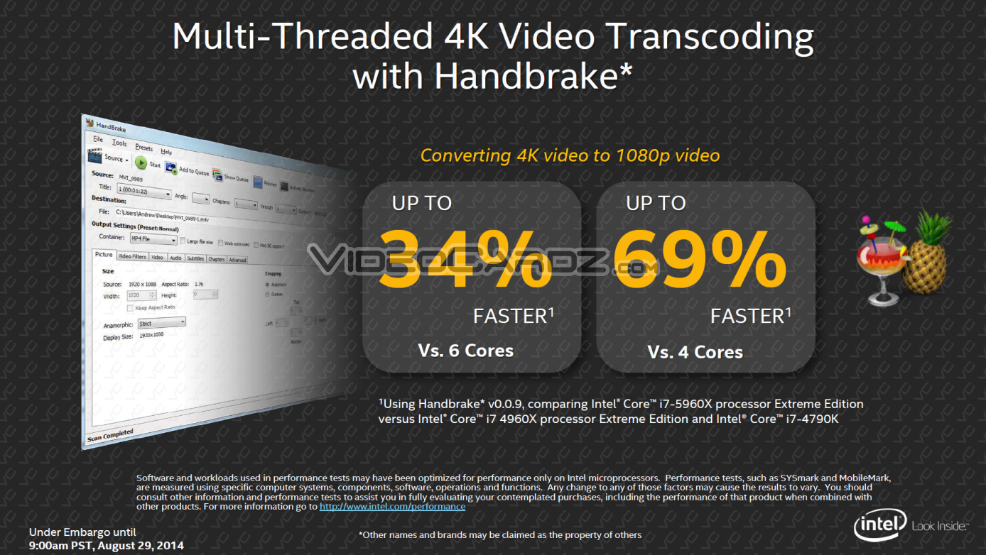
In terms of raw performance, the Core i7-5960X is around 20% faster in terms of 4K Video Editing, 32% faster in 3D rendering and 14% faster in games and AI processing compared to the last generation Core i7-4960X CPU that is the flagship Ivy Bridge-E offering. The models will be available with Intel’s TS13X liquid cooler which has been in the market since the first generation of Sandy Bridge-E processors and is priced in between $85-$100 and compatible with LGA 2011-3, LGA 2011, LGA 1366 and LGA 115* platforms.

Thayn3 over at coolaler forums configured a test setup for the Haswell-E platform which includes a Gigabyte X99 Gaming G1 WiFi motherboard, 16 GB of G.Skill Ripjaws IV memory operating at 3000 MHz CL15, two GTX Titan Black graphics cards, two Sandisk Extreme Pro 256 GB SSDs in Raid 0 and a Corsair H110 AIO closed loop liquid cooler. In stock performance numbers, the Core i7-5960X scored 18978 MB/s / 16573 MB/s / 16475 MB/s and 150.0 ns in Memory Copy/Read/Write/Latency benchmarks through MaxxMem 2. In Cinebench, the chip scored 1270 CPU marks in multi-threaded performance compared to 1096 on the Core i7-3930K and 822 on the Core i7-4770K.

The used also overclocked the chip to 4.0 GHz at just 1.200V (fixed voltage) which resulted in a Cinebench score increase to 1508 from 1270 and in HyperPI, the chip was able to finish 1M calculations in just 14.555 seconds. Surprisingly, the temperatures during both stock and overclocked runs was pretty decent for the chip, running at a maximum temperature of 55C at 4.0 GHz and 45C at the stock clock speeds. Following is a run down of the scores:

CineBench R15 (CPU Multithreaded Performance):

  • Intel Core i7-5960X @ 4.0 GHz: 1508
  • Intel Core i7-5960X @ 3.0 GHz: 1270
  • Intel Core i7-3930K @ 3.3 GHz: 1096
  • Intel Core i7-4770K @ 4.4 GHz: 822

Hyper PI and MaxxMem Performance:

  • Intel Core i7-5960X @ 4.0 GHz Maxmemm: 18978 MB/s / 16573 MB/s / 16475 MB/s and 150.0 ns
  • Intel Core i7-5960X @ 4.0 GHz HyperPi: 14.555 Seconds

We also have a surprise for you, a few days ago, we found a validation of the Core i7-5960X which was running at 6.2 GHz on LN2 overclock with the X99S SLI Plus motherboard. You can find it below:
Intel Core i7-5960X 6.25 GHz Overclock

Intel Core i7-5960X Benchmarks (Courtesy of Coolaler):
Intel Core i7-5960X Cinebench R15 BenchmarkIntel Core i7-5960X HyperPi BenchmarkIntel Core i7-5960X MaxxMem Performance


If you want to contact RDT please feel free to call between the hours of 9am-8pm AEST. deon@robertsondt.com Ph: 0426279566 or visit https://www.facebook.com/rdtaus

Wednesday, 27 August 2014

Intel Skylake-S iGPU Will Have DirectX12 and 4K Resolution Support

We have received an update on the Skylake-S iGPU front from Fudzilla.com. Fudzilla has been rock solid about Intel leaks in the past, so I won’t be tagging this as a rumor. It looks like the Skylake-S CPUs will have DirectX12 compatibility and 4K resolution support. iGPUs have really come around in the past few years (we can thank AMD for the competition) and this is great news for OEMs and users who rely only on the iGPU.Intel Broadwell and Skylake Platform

DirectX 12 and 4K Resolution Support to be Featured in Intel Skylake-S

We have already released quite a lot of Info on Skylake-S including the fact that it will be launching alongside Broadwell-K and will consist entirely of locked multiplier CPUs on release. Skylake-S is ofcourse based on 14nm and will feature optimized architecture with the downside of no unlocked multiplier. As before we have already covered details regarding Skylake-S’s iGPU before but we have a few things to add to that. For e.g the fact that Skylake-S integrated graphics will be fully compatible with DX12. Whether or not it will support all the hardware based functions of DirectX 12 is unknown. But looking at the time frame of the launch, I think this is a real possibility.
The latest version of Open GL (5.x) will also be supported alongside the latest version of Open CL (2.x). HEVC codecs VP8 and VP9 will be supported. Resolution up to 4096×2304 (4K) which is a 16:10 aspect ratio. Ofcourse there is no way on this earth that you will be able to play any modern game at that resolution, but the iGPU should suffice for 4k video playback and general screen management. This will be coupled with Intel’s 100 Series chipset, this will be led by the Intel Z170 Chipset. It will support DMI and PCIe 3.0 up to 8GT/s. The source also mentions that this is all in time for 20nm GPUs that are coming in mid-2015.


Source: http://wccftech.com/intel-skylake-s-igpu-directx12-4k-resolution-support/#ixzz3BgH6pbFh


If you want to contact RDT please feel free to call between the hours of 9am-8pm AEST. deon@robertsondt.com Ph: 0426279566 or visit https://www.facebook.com/rdtaus

Tuesday, 26 August 2014

RDT's 4K Custom Rendering Machines

RDT offers the best custom PC/Hackintosh's in Melbourne. If you are looking at upgrading your business or personal computer and wanting some more grunt then RDT is what you need. 

With RDT's quality assured builds you will be incredibly happy, we pride ourselves on working as close to our clients as possible on a friendly and personal basis. Our builds use only the best quality and locally purchased. Don't get scammed by cheap counter fits and dodgy workmanship. 

With RDT 4K editing builds starting from $1,599 AU. You are open to many options for upgrades depending on your line of work. 

If you want to contact RDT please feel free to call between the hours of 9am-8pm AEST. deon@robertsondt.com Ph: 0426279566 or visit https://www.facebook.com/rdtaus or visit www.robertsondt.com 

***Purchases made through PayPal will incur a 2.4% Fee***


If you want to contact RDT please feel free to call between the hours of 9am-8pm AEST. deon@robertsondt.com Ph: 0426279566 or visit https://www.facebook.com/rdtaus

Monday, 25 August 2014

Intel Haswell-E i7 5960X, i7 5930K and i7 5820K US Pricing

While we are very close to Second Generation Maxwell architecture announcement, Intel is also preparing for a big launch on August 29th. Today we are going to talk about CPUs.
Haswell-E is just around the corner, and I know many of are planning to replace both CPU and GPU at the same time. For that reason I thought you might be interested in pricing of the new platform.
Intel i7 / X99 Haswell-E pricing:
  • Intel Core i7 5960X 8C/16HT – 40-lane PCI-Express support (x16 + x16 + x8) — $999 US
  • Intel Core i7 5930K 6C/12HT – 40-lane PCI-Express support (x16 + x16 + x8) — $583 US
  • Intel Core i7 5820K 6C/12HT — 28-lane PCI-Express support (x16 + x8 + x4) —– $389 US
Intel i7 5820K looks like sweet spot for single high-end graphics card owners. Now, if you own two high-end cards, or you’re planning to upgrade your rig to CrossFire or SLI, then you should think about i7 5930K, as it will offer two x16 PCI-E lanes. It probably won’t change much in terms of performance, but it’s always good to know you are squeezing all juice from your beloved cards.
My first ever CPU was Intel 486DX and I still use it to this day… as a key chain…
Enjoy the slides.
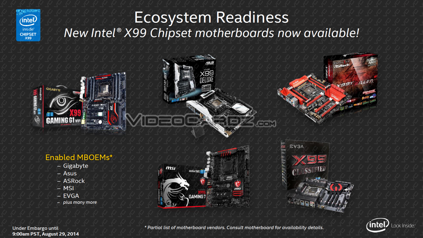
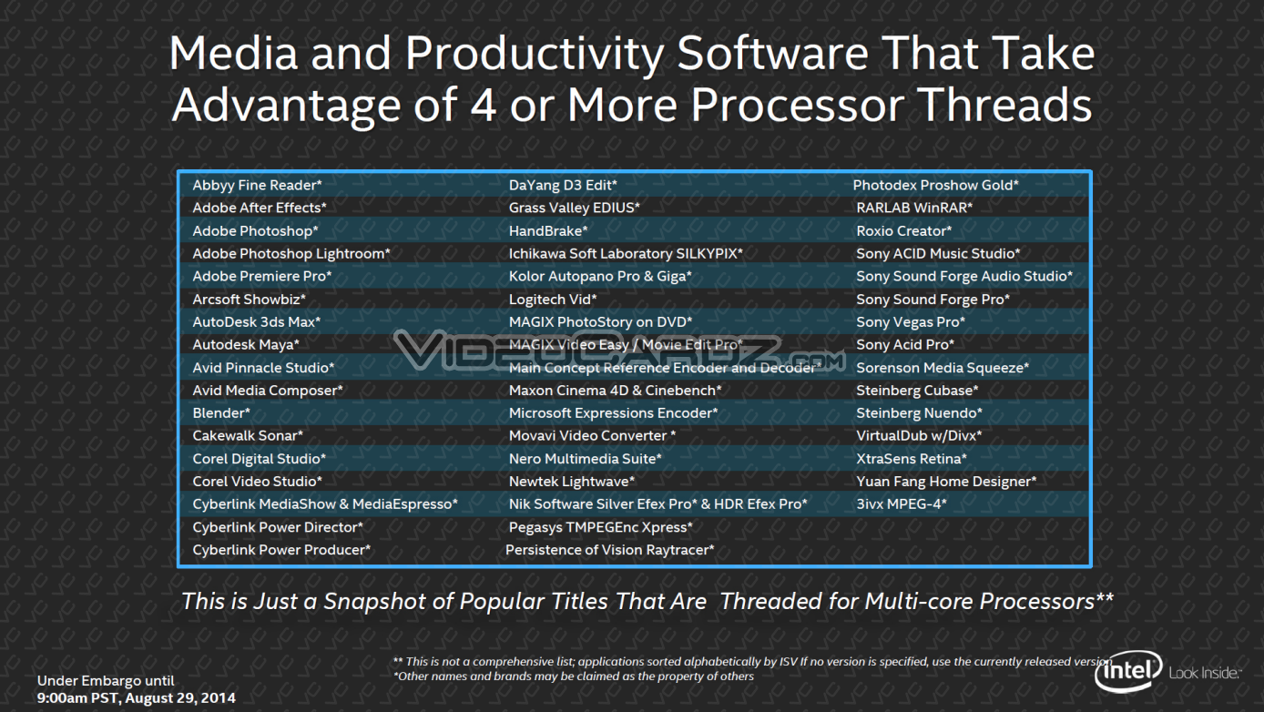
Intel HaswellE-E VideoCardz_Com Press Deck (1) Intel HaswellE-E VideoCardz_Com Press Deck (2) Intel HaswellE-E VideoCardz_Com Press Deck (3) Intel HaswellE-E VideoCardz_Com Press Deck (4) Intel HaswellE-E VideoCardz_Com Press Deck (5) Intel HaswellE-E VideoCardz_Com Press Deck (6) Intel HaswellE-E VideoCardz_Com Press Deck (7) Intel HaswellE-E VideoCardz_Com Press Deck (8) Intel HaswellE-E VideoCardz_Com Press Deck (9) Intel HaswellE-E VideoCardz_Com Press Deck (10) Intel HaswellE-E VideoCardz_Com Press Deck (11) Intel HaswellE-E VideoCardz_Com Press Deck (12) Intel HaswellE-E VideoCardz_Com Press Deck (13) Intel HaswellE-E VideoCardz_Com Press Deck (14) Intel HaswellE-E VideoCardz_Com Press Deck (15) Intel HaswellE-E VideoCardz_Com Press Deck (16) Intel HaswellE-E VideoCardz_Com Press Deck (17)
If you want to contact RDT please feel free to call between the hours of 9am-8pm AEST. deon@robertsondt.com Ph: 0426279566 or visit https://www.facebook.com/rdtaus