Showing posts with label graphics card. Show all posts

Sunday, 18 January 2015

ASUS, EVGA and ZOTAC GeForce GTX 960 pictured

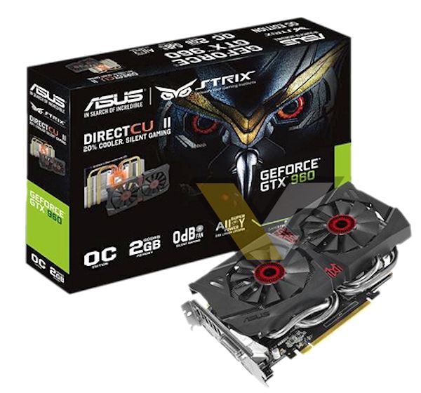
ASUS STRIX GeForce GTX 960 OC (STRIX-GTX960-DC2OC-2GD5)

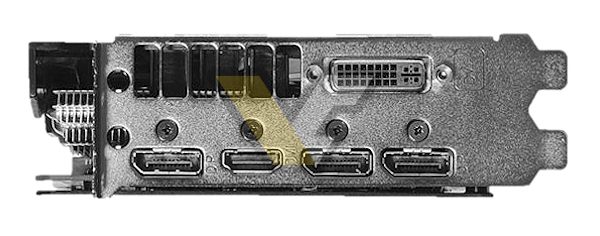
ASUS STRIX GTX 960 is an overclocked card equipped with DirectCU II cooler. The GTX 960 will feature 0 dB technology, the same technology that is available in all STRIX graphics cards. The card itself is a rather tiny, probably best fitted for mini-ITX builds. It does look like STRIX GTX 750 Ti, except it has more display connectors.
ASUS STRIX GTX 960 2GBASUS STRIX GTX 960 2GB angle
ASUS STRIX GTX 960 2GB bracket

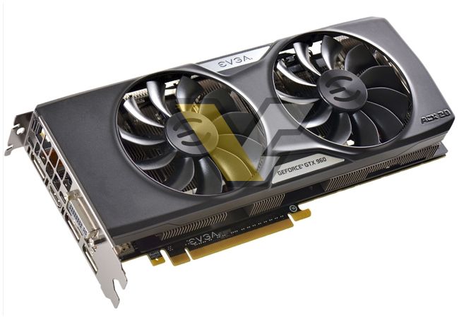
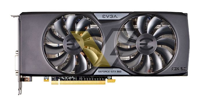
EVGA GeForce GTX 960 Superclocked

For the fans of ACX 2.0 cooling (there are any here?) EVGA brings new Superclocked GTX 960 (and some other models no one cares about).
The GTX 960 Superclocked is powered with through single 8-pin power connector. It has a full cover base plate, two heat sinks connected to each other with three copper heat pipes.  The ACX 2.0 has two 80mm 11-blade fans. I don’t know how what are the clocks yet, but I will keep you updated.
EVGA GTX 960 SSC (2)EVGA GTX 960 SSC (1) EVGA GTX 960 SSC (3)

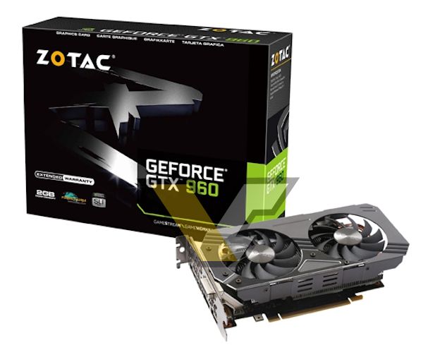
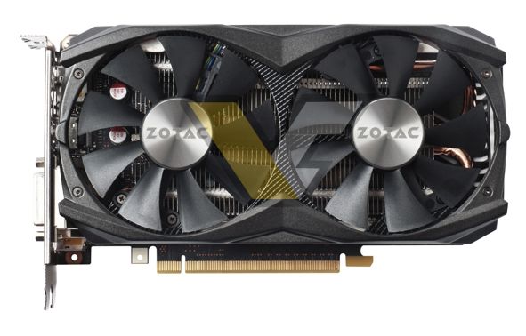
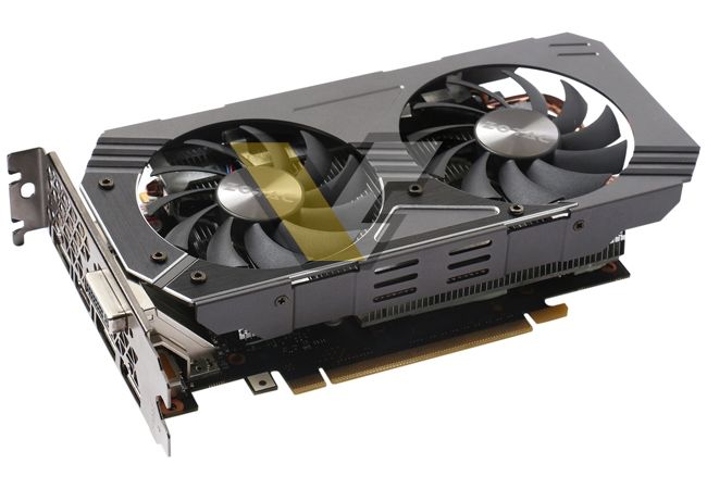
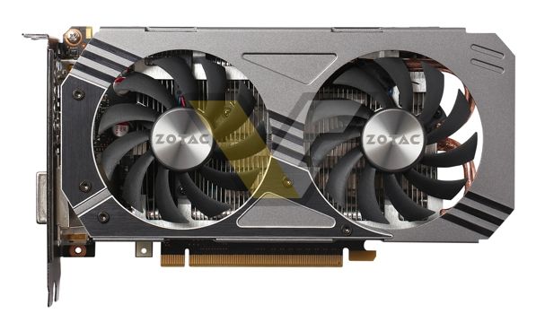
ZOTAC GeForce GTX 960

ZOTAC has four GTX 960 cards in the making. These cards only feature two designs and optional factory-overclocking. The first card is simply called ZOTAC GTX 960. You can actually get the same cooler with GTX 970, but I suppose it’s more suitable for this card anyway. ZOTAC’s GTX 970 features one 6-pin connector. The PCB is actually shorter than the dual-fan cooler itself.
The overclocked model based on this design will ship with 1177 / 1240 MHz clocks.
ZOTAC GeForce GTX 960 (3)ZOTAC GeForce GTX 960 (1)ZOTAC GeForce GTX 960 (2)

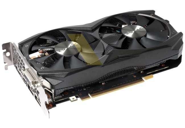
ZOTAC GeForce GTX 960 AMP!

Here is my favorite model so far. The dual-fan AMP! edition. More powerful cards like 970 and 980 are available with triple-fan edition of the same cooling system. The GTX 960 however, is not as demanding as GM204-powered cards, thus only 2 fans are required.
While it does look nice, it only has one 6-pin power connector, so I’m not sure if it can live up to the expectation of overclockers. It does however have a backplate, so if you’re into those kind of things, this could be the perfect card for you. The AMP! model has GPU clocks of 1266 / 1329 MHz.
ZOTAC GeForce GTX 960 AMP (3)ZOTAC GeForce GTX 960 AMP (1)
ZOTAC GeForce GTX 960 AMP (2)
Source: http://videocardz.com/54374/asus-evga-and-zotac-geforce-gtx-960-pictured
If you want to contact RDT please feel free to call between the hours of 9am-8pm AEST. deon@robertsondt.com Ph: 0426279566 or visit https://www.facebook.com/rdtaus
Wednesday, 12 November 2014

AMD’s Radeon R9 390X ‘Fiji XT’ may feature 4096 SPs, extreme memory bandwidth

Advanced Micro Devices’ next-generation graphics processing unit is still several months away, but it looks like it is worth waiting. According to unofficial information from SiSoft Sandra benchmark’s database, the forthcoming GPU features unprecedented compute horsepower as well as uses multi-layer high-bandwidth memory with extreme bandwidth.
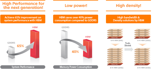
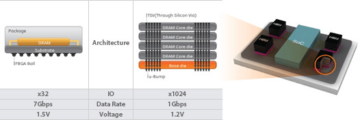
If the listing in Sandra’s database is correct and really describes a prototype of the Radeon R9 390X “Fiji XT” graphics card, the next-generation offering from AMD will feature 4096 stream processors (SPs) (which, in case of the GCN 1.2 architecture, means 64 compute units and 256 texture units) and 4096-bit memory bus. The memory sub-system will rely on SK Hynix’s stacked high bandwidth memory (HBM) chips with 1024-bit input/output interface (compliant with the Wide IO standard).
amd radeon hd 7000 artwork AMD’s Radeon R9 390X ‘Fiji XT’ may feature 4096 SPs, extreme memory bandwidth
The graphics card allegedly sports only 4GB of memory since the first-generation HBM features 2Gb DRAM dies and comes in 1GB memory devices, reports Wccftech. Only the second-generation HBM is expected to use 8Gb dies and therefore support 4GB and 8GB configurations.
If AMD’s Radeon R9 390X actually uses four first-generation HBM DRAM chips with 4096-bit memory bus operating at 1.25GHz, then the actual memory bandwidth the graphics card will sport will be whopping 640GB/s.
sk hynix hbm AMD’s Radeon R9 390X ‘Fiji XT’ may feature 4096 SPs, extreme memory bandwidth
With 4096 stream processors and amount of bandwidth never before seen on a single-chip graphics cards, the Radeon R9 390X will be the fastest graphics adapter on the market. In fact, with such extreme amount of stream processors, it will clearly leave behind any graphics solution based on Nvidia Corp.’s GM200 graphics processing unit.
sk hynix hbm 1 AMD’s Radeon R9 390X ‘Fiji XT’ may feature 4096 SPs, extreme memory bandwidth
While performance-wise the Radeon R9 390X “Fiji XT” seems to be very powerful, it remains to be seen how expensive will it be. New types of memory tend to cost a lot. Moreover, given that memory devices have to be placed on the same piece of substrate with the GPU, the whole graphics card has to be redesigned.
Source: http://www.kitguru.net/components/graphic-cards/anton-shilov/amds-radeon-r9-390x-fiji-xt-may-feature-4096-sps-extreme-memory-bandwidth/
If you want to contact RDT please feel free to call between the hours of 9am-8pm AEST. deon@robertsondt.com Ph: 0426279566 or visit https://www.facebook.com/rdtaus
Sunday, 28 September 2014

GeForce GTX 970 2-way SLI

GeForce GTX 970 2-way SLI

We review that lovely GeForce GTX 970 but this time in a 2-way SLI setup. In this review we'll run the standard benchmarks, but we will also have a good look at Ultra HD gaming performance as well as a micro stuttering analysis with the help of FCAT. In this article we'll be looking at 2-way SLI performance from a single monitor point of view, so ideally with so much horsepower a WQHD resolution (2560x1440/1600) is the monitor you need to have to be able to compare to what SLI would do for you on your setup, preferably even Ultra HD of course. You will notice great performance increases with 2-way SLI as the cards scale nicely with so much horsepower.
With that in the back of our mind we created a second segment in this article. For the second part of this article we'll take it up a notch and look into Ultra High-resolution gaming as we hook up an Ultra High Definition monitor. While Full HD (1920x1080/1200) and WHQL (2560x1440) have become the industry standard within the display industry, enthusiasts will never settle for just standard and are always looking for the next big innovation in technology. Ultra HD gaming is the next evolution in immersion that gamers have been waiting for. Commonly addressed as Ultra HD, UHD or 4K, this new resolution refers to the ultra-high resolutions with approximately 4000 horizontal pixels. Ultra HD resolution also has four times the number of pixels of a typical 1920x1080 resolution. It will be interesting to find out how the GeForce GTX 970 cards will handle such extreme resolutions. Considering its nice 4 GB framebuffer but  slightly dimmed memory bandwidth yet hefty GPU clocks, it's looking quite alright I'd say! With UHD (Ultra High Definition Gaming) becoming rapidly popular we'll test multiple multi-GPU setups on such a monitor. Next to that we'll perform FCAT tests to see where AMD is in Autumn anno 2014 in terms of micro-stuttering and frame pacing.
Join us in this review where we'll once again look at everything. As if you figured just one card would be interesting, you have no idea what's coming at you with two cards. 


Read More here: http://www.guru3d.com/articles-pages/geforce-gtx-970-sli-review,1.html

If you want to contact RDT please feel free to call between the hours of 9am-8pm AEST. deon@robertsondt.com Ph: 0426279566 or visit https://www.facebook.com/rdtaus
Thursday, 28 August 2014

Nvidia to skip GeForce GTX 800 series, to introduce GeForce GTX 970, GTX 980 in mid-September

Although it was expected that Nvidia Corp. would release its new GeForce GTX 800-series graphics cards for desktops this September and October, the company has decided to skip the GeForce 800 family for desktop PCs and jump straight to the GeForce 900 line of products.
Model numbers of modern central processing units and graphics processing units have been criticized criticized for years since in many cases they barely reflect performance and positioning of products and in many cases cannot even determine their generation. At present Nvidia offers high-end GeForce GTX 700-series of products for desktop computers. At the same time, the company sells GeForce GTX 800M family of products for notebooks. What is rather confusing is that both lineups – the GTX 700 and the GTX 800M – are based on similar chips powered by the Kepler architecture.
In a bid to avoid confusion with its upcoming families of graphics processing units for desktop and mobile computers, Nvidia decided to sell its products powered by the second-generation Maxwell GPUs code-named GM200, GM204 and other under the GeForce 900 moniker, reportsVideoCardz.
nvidia artwork1 Nvidia to skip GeForce GTX 800 series, to introduce GeForce GTX 970, GTX 980 in mid September
As a result, Nvidia is now expected to formally introduce the GeForce GTX 970 and the GeForce GTX 980 graphics cards on the 19th of September, 2014. The GeForce GTX 960 is projected to arrive sometime in October.
Nvidia did not comment on the news-story.
Source: http://www.kitguru.net/components/graphic-cards/anton-shilov/nvidia-to-skip-geforce-gtx-800-series-to-introduce-geforce-gtx-970-gtx-980-in-mid-september/
If you want to contact RDT please feel free to call between the hours of 9am-8pm AEST. deon@robertsondt.com Ph: 0426279566 or visit https://www.facebook.com/rdtaus
Monday, 25 August 2014

Sapphire launched R9 285 ITX Compact display card

Shortly new GPU, AMD's top partners that delivered small design display card.
Introduction of compact design for the now popular ITX chassis performance level graphics card is nothing new. But this Radeon R9 285 published but two days, we saw ITX special design card from Sapphire's - R9 285 ITX Compact Edition.
115c 665x757 Small hosts optimization, Sapphire launched R9 285 ITX Compact display card
Radeon R9 285 ITX Compact Edition, a length of about about 17CM, standard 2-slot thickness design, the radiator part of the grounds is a copper base aluminum fins figure looks, coupled with 10CM fan heat pipe design. Power part is the use of two PCIe 6PIN as the power input. GPU of course, is to use the latest Tonga GPU, has 1792SP's GCN 1.1 architecture, with the 256-bit of 2GB GDDR5, the clock part 918Mhz / 5.5GHz, Sapphire will launch a small margin for overclocking OC edition.
115b 665x474 Small hosts optimization, Sapphire launched R9 285 ITX Compact display card
Other parts, R9 285 ITX Compact Edition will be with a push switch, can switch to Legacy mode VGA BIOS and UEFI mode is fully optimized for UEFI BIOS. Output interface has two mini-DisplayPort 1.2, HDMI 1.4a and Dual-Link DVI.
115a 665x641 Small hosts optimization, Sapphire launched R9 285 ITX Compact display card

If you want to contact RDT please feel free to call between the hours of 9am-8pm AEST. deon@robertsondt.com Ph: 0426279566 or visit https://www.facebook.com/rdtaus
Tuesday, 19 August 2014

Nvidia already testing GM200 graphics processor

Nvidia Corp. recently shipped the first samples of graphics cards based on the code-named GM200 graphics processing units (GPUs) to its developers in India. This confirms that the company already taped out the new GPU and got the first samples of the chip from the fab. Theoretically, Nvidia could launch commercial graphics cards based on the GM200 already later this year.
According to Zauba.com database, which monitors imports and exports to and from India, where high-tech companies employ a lot of software developers, Nvidia shipped the first graphics cards based on the GM200 to its developers in early July. Recently the company imported the so-called “customer samples” of graphics boards powered by the GM200 GPU to India, which may be an indicator that the new graphics processor is approaching its commercial launch, reports WccfTech.
Based on the data from Zauba, Nvidia first imported GM204-based graphics cards to its Indian developers in early June. As reported, the GeForce GTX 860/870/880 graphics cards based on the GM204 will be rolled-out in late September, or early October. Therefore, it takes Nvidia around four months to finalize a product after it ships its first test samples to Indian developers. It is possible that Nvidia officially launches its GM200-based solutions in November, if everything goes as planned.
nvidia artwork iron Nvidia already testing GM200 graphics processor
Nvidia’s GM200 graphics processing unit is believed to be based on the second-generation Maxwell architecture and is reportedly designed to replace the GK110 graphics processor as the world’s most advanced GPU. The chip is reportedly made using 28nm process technology.
It is noteworthy that graphics cards based on the GM204 and the GM200 carry A1 revisions of the chip. Typically Nvidia launches commercial products with A2 revisions. The status of the latter is completely unknown.

Source: http://www.kitguru.net/components/graphic-cards/anton-shilov/nvidia-already-testing-gm200-graphics-processor/
If you want to contact RDT please feel free to call between the hours of 9am-8pm AEST. deon@robertsondt.com Ph: 0426279566 or visit https://www.facebook.com/rdtaus
Saturday, 9 August 2014

Nvidia GeForce GTX 800: what to expect from its specs?

Nvidia Corp. and its partners among makers of graphics cards are expected to release the next-generation GeForce GTX 800-series solutions sometimes in October (or even late September), according to multiple reports. But while the new graphics solutions are just a couple of months away, it is completely unknown what to expect from them. We decided to analyze what we do know for sure about the GM204, the graphics processor that will power the new cards, and what kind of specifications and performance should we expect.
nvidia artwork iron Nvidia GeForce GTX 800: what to expect from its specs?
Facts we know for (almost) sure
While there are not a lot of reliable facts from sources close to Nvidia available at the moment, here is what we have found so far about the GM204 and what either is trustworthy or, at least, looks trustworthy:
  • Nvidia GM204 is based on the code-named Maxwell architecture;
  • Nvidia GM204 is made using 28nm process technology (given that multiple sources said that the GM204 is a 28nm GPU, it is most probably a fact);
  • Nvidia GM204 has die size of around 300mm² (we’ve seen the chip, we’ve discussed that performance GPUs from Nvidia feature about 300mm² die size);
  • Nvidia GM204 most likely 256-bit memory bus (we’ve seen a GM204-based card, it features 16 GDDR5 memory chips (with 16-bit or 32-bit interfaces), hence, given the size of the chip, 256-bit memory bus is a more likely option);
While we have no idea about exact specifications of the GM204, we do know specifications of the GM107 thanks to the official launch of the GeForce GTX 750-series GPUs earlier this year and hence we know something about the Maxwell architecture in general.
Maxwell architecture
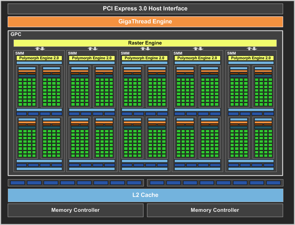
Nvidia’s graphics processors consist of several key building blocks: main scheduler/dispatch processor (which Nvidia calls GigaThread Engine), GPCs [graphics processing clusters], SMMs [streaming multiprocessor module], ROPs [raster operating units], cache, memory controllers.
GeForce GTX 750 Ti Block Diagram FINAL Nvidia GeForce GTX 800: what to expect from its specs?
A block diagram of Nvidia’s GM107 graphics processing unit.
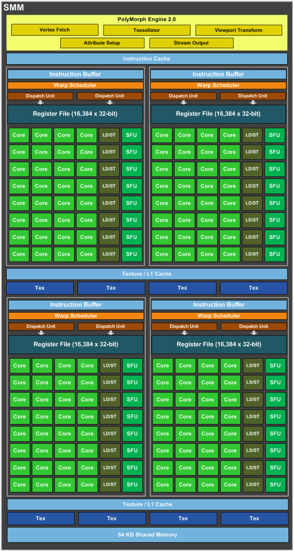
The GM107 graphics processor based on the first-gen Maxwell architecture features one GPC unit, 16 ROPs (in two blocks,), 2MB L2 cache and two 64-bit memory controllers. The GPC of the GM107 consists of five SMMs. Each first-gen Maxwell SMM features its own PolyMorph Engine 2.0 unit (one vertex fetch, one tessellator, one viewport transform, one stream output, etc.) and is divided into four blocks with their own control logic (instruction buffer, warp scheduler, dispatch unit), a register file, two texture units (TUs) and 32 stream processors (SPs) (thus, each SMM features 128 SPs, 8 TUs, etc.).
nvidia maxwell smm 546x1024 Nvidia GeForce GTX 800: what to expect from its specs?
A block diagram of a Maxwell SMM
According to Nvidia, thanks to better programmability of each block within an SMM and higher utilization rate of each stream processors, the company increased the peak performance per stream processor by 35% when compared to the SPs in its chips built with the previous generation Kepler architecture. Therefore a Maxwell-based GPU with equal (or more or less equal) amount of stream processors with a Kepler-based GPU will perform around 35 per cent better.
Nvidia’s GM107 graphics processing unit features 640 SPs, 40 TUs, 16 ROPs, 2MB cache and a 128-bit memory controller. The chip contains 1.87 billion of transistors and has 148mm² die size.
What Nvidia needs from GM204?
Since the GM204 is a successor to the GK104 graphics processor (GeForce GTX 670, 680, 760 and 770) made using the same 28nm process technology, Nvidia cannot really expect it to outperform its predecessor by two times or something like that. Realistically, Nvidia needs to tangibly outperform the best GK104 by around 30 to 40 per cent. It is impossible that a 300mm² Maxwell chip could beat the GK110 GPU with 2880 stream processors (which die size is 551mm²), hence, it is not a target that the GM204 should achieve.
Possible GM204 configurations
Each architecture can be scaled to offer better performance or lower power consumption. Let’s try to assume how Nvidia could scale the GM107’s architecture to offer better performance with the GM204 while maintaining around 300mm² die size.
The easiest way to double performance of the GM107 is to double the amount of virtually everything inside: GPC, ROPs, cache, memory controllers. Such a chip would have 1280 stream processors, 80 texture units, 32 ROPs and a 256-bit memory bus. The GPU would never outperform the GK104 (1536 SPs, 128 TUs, 32 ROPs, etc.) significantly and in many cases will be behind the older solution. Therefore, it is unlikely that Nvidia will take this route. Moreover, such a chip would be significantly smaller than 300mm² since not all elements of the chip have to be doubled.
What Nvidia did with GK110 compared to the GK104 architecturally (at least when it comes to organization of execution units) was the increase of the amount of SMs [streaming multiprocessor] per GPC from two to three. The same approach could be used for the GM204 too. Nvidia could expand GPC to six SMMs and then double the amount of GPCs (and ROPs, cache, memory controllers) per chip. Such a GPU would feature 1536 SPs, 96 TUs, 32 ROPs as well as a 256-bit memory bus and could offer up to 35 per cent higher performance compared to the GK104 at the same clock-rate. The die size of such chip would probably be around 300mm², but since we do not know anything about exact sizes of the GM107’s elements, we cannot be 100 per cent sure.
Theoretically, Nvidia could put six blocks into each SMM (thus increasing the amount of SPs per SMM to 192), then double the amount of GPCs (along with ROPs, cache, memory controllers) per GPU. If Nvidia manages to do this, then the final chip would feature 1920 SPs, 120 TUs, 32 ROPs and a 256-bit memory controller. Would that all fit into a 300mm² die area? Possibly. However, since this fundamentally changes the architecture of the SMM, this could also affect efficiency of Maxwell architecture in general. Therefore, the expansion of GPC to seven SMMs (and doubling the amount of GPCs, etc.) sounds more realistic (the GPU would have 1792 SPs, 112 TUs, 32 ROPs, 256-bit memory bus).
Final words
While chip designers can do many unexpected things and sometimes even wonders, they cannot overrule the laws of physics. Engineers will not be able to squeeze 3200 stream processors into the GM204 that is made using 28nm process technology and has die size of around 300mm². Therefore, the most logical configurations of the fully-fledged GM204 (the GeForce GTX 880) are as follows:
  • 1536 SPs, 96 TUs, 32 ROPs, 256-bit memory bus
  • 1792 SPs, 112 TUs, 32 ROPs, 256-bit memory bus
  • 1920 SPs, 120 TUs, 32 ROPs, 256-bit memory bus
Of course, these specifications may be wrong as well…
Nvidia did not comment on the news-story.

Source: http://www.kitguru.net/components/graphic-cards/anton-shilov/nvidia-geforce-gtx-800-what-to-expect-from-its-performance-and-specs/
If you want to contact RDT please feel free to call between the hours of 9am-8pm AEST. deon@robertsondt.com Ph: 0426279566 or visit https://www.facebook.com/rdtaus

Friday, 8 August 2014

Nvidia Quadro New Series Lineup Arriving on 12th August – K420, K620, K2200, K4200 and K5200 Confirmed

Our Japanese colleagues over at Hermitage Akihabara have revealed the launch date and the lineup of the new Quadro series. I will not be tagging this one as rumor, since their leaks have been spot on in the past. The new series (so far) will consist of Quadro K420, K620, K2200, K4200 and K5200 and will paper launch on the 12th of this month with SKUs being available soon after. It is unknown how many of the lineup is Maxwell and how much is Kepler, though speculation on the same certainly exists.NVIDIA Quadro K6000 GPU

Nvidia Quadro K420, K620, K2200, K4200 and K5200 Launching on 12th August

Now I know the first thing anyone will ask is, are they Maxwell? Well, the lineup will almost certainly have Maxwell SKUs but it is just as certain that there are going to be Kepler parts as well. What is arguable, is the number of Maxwell Counterparts. Now we did have some previously revealed data on the lineup from driver changelogs andbased on that, we are looking at 2 Maxwells. Both of them are allegedly, GM107 cores. That would also make these Quadros the 750/750Ti’s of the professional world, with the actual Flagship and the equivalent of the Quadro K6000 coming later. Now The 5200 is supposedly based on a Kepler core, which makes it an unsuitable replacement for the K6000. A GM204 Quadro K6000 replacement, would be perfect for Nvidia’s value chain, unless they decide to go with GM200 directly. Here is the lineup leaked thanks to Laptop Video2Go and confirmed by HA:

  • NVIDIA Quadro K420 (NVIDIA_DEV.0FF3 )
  • NVIDIA Quadro K/M 620 (NVIDIA_DEV.13BB) Speculated GM107 Core
  • NVIDIA Quadro K/M 2200 (NVIDIA_DEV.13BA) Speculated GM107 Core
  • NVIDIA Quadro K4200 (NVIDIA_DEV.11B4)
  • NVIDIA Quadro K5200 (NVIDIA_DEV.103C)

Now interestingly the source mentions doubling of memory, and I am not entirely sure what to make of that. Are we looking at double the memory of the older generation? or what? But since the launch is just a few days away, it is kind of pointless to speculate at this point. However, I would like to pick a bone with Nvidia’s nomenclature. The first alphabet depicts the architecture. So naming a Maxwell card ‘K’xxx/x is absurd, but Nvidia  would have trouble switching over to the ‘M’ letter, not without utterly messing up the system. Here is an example, the mobile variants usually have the m suffix, so the technically correct naming of a randomly chosen Maxwell card would be Quadro M2200m but that is semantic redundancy and would be marketing folly.  Green can always decide to name the mobile series differently but that would just be a blunder over a blunder. Either way I would be very interested to see how Nvidia names their flagship professional GPU.

Source: http://wccftech.com/nvidia-quadro-series-arriving-12th-august-k420-k620-k2200-k4200-k5200-confirmed/#ixzz39qFBAql1

If you want to contact RDT please feel free to call between the hours of 9am-8pm AEST. deon@robertsondt.com Ph: 0426279566 or visit https://www.facebook.com/rdtaus

Wednesday, 6 August 2014

NVIDIA Graphics Drivers OS X 10.9.4

Name:  351px-Nvidia_logo.svg.png
Views: 9724
Size:  11.4 KB
NVIDIA has released their alternate graphics drivers for OS X Mavericks 10.9.4. These are separate from the drivers Apple ships as standard, and should be considered experimental. These drivers have been known to solve OpenCL issues with certain applications, as well as providing better native GPU power management for certain devices. If you've installed the drivers before, you may get a notification to update to the 10.9.4 drivers from the built in System Preferences pane. 

Click image for larger version. 

Name: Screen Shot 2014-07-01 at 8.47.09 AM.png 
Views: 10442 
Size: 60.4 KB 
ID: 97397

NVIDIA Web Driver 334.01.02f02
http://www.nvidia.com/download/drive...px/76505/en-us 

Click image for larger version. 

Name: Screen Shot 2014-07-01 at 8.54.32 AM.png 
Views: 10263 
Size: 134.1 KB 
ID: 97395


How to Install the Web Drivers: 
In order to flag the alternate drivers on a CustoMac using Chameleon/Chimera, you must install the package and also add the flag manually to the chameleon.org.Boot.plist. If you use Clover, you can toggle back and forth using the standard menubar or system preference pane. 

1. Open Finder
2. Navigate to /Extra/org.chameleon.Boot.plist
3. Open in TextEdit
4. Add nvda_drv=1 to Kernel Flags as shown:

Example Usage:

Code:
<key>Kernel Flags</key>
<string>nvda_drv=1</string>
5. Save and reboot

You should be on the new NVIDIA drivers. 

Source: http://www.tonymacx86.com/graphics/135997-nvidia-releases-alternate-graphics-drivers-10-9-4-334-01-02f02.html

If you want to contact RDT please feel free to call between the hours of 9am-8pm AEST. deon@robertsondt.com Ph: 0426279566 or visit https://www.facebook.com/rdtaus
Tuesday, 5 August 2014

Gigabyte confirms Nvidia GeForce GTX 880 launch

A representative for Gigabyte Technology has confirmed that the company plans to introduce its next-generation Nvdia GeForce GTX 880-based graphics cards this fall. The company even said that the boards will use custom coolers, which may mean that they will also be factory overclocked.
In an interview with a Chinese web-site a graphics marketing director at Gigabyte Technology said that the GeForce GTX 880 G1 Gaming graphics card would be released in late September, or early October, 2014. The timeframe was confirmed earlier by unofficial sources, hence, it is likely that it is correct.
Gigabyte G1 Gaming GeForce GTX 880 graphics card is projected to feature improved design (it is unclear whether the card will rely on Gigabyte’s own printed-circuit board, or will feature a reference PCB along with some improvements) with a proprietary cooling system, LED lights, metal back-plate and so on. It is highly-likely that the graphics board will be factory overclocked and will be faster than competitors.
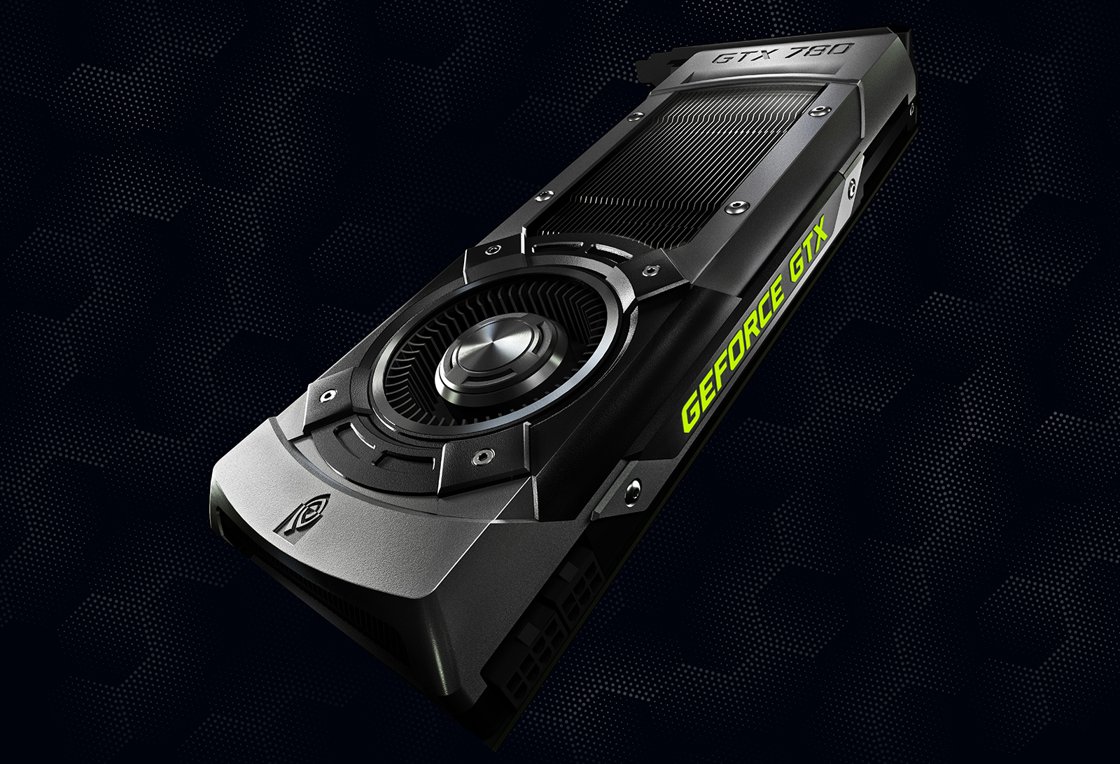
nvidia geforce gtx 780 art 1024x698 Gigabyte confirms Nvidia GeForce GTX 880 launch this fall
The fact that Nvidia will allow Gigabyte and other makers to pre-overclock the GeForce GTX 800-series graphics card means that the solutions will be positioned exactly as expected: as high-end gaming-class graphics boards. It looks like the GeForce GTX Titan-series products will remain Nvidia’s highest-performing graphics boards this year.
Nvidia GeForce GTX 800-series graphics cards will be based on the GM204 graphics processing unit, which belongs to the second-generation Maxwell family of GPUs. The GM204 is projected to be made using 28nm process technology.
Source: http://www.kitguru.net/components/graphic-cards/anton-shilov/gigabyte-confirms-nvidia-geforce-gtx-880-launch-this-fall/
If you want to contact RDT please feel free to call between the hours of 9am-8pm AEST. deon@robertsondt.com Ph: 0426279566 or visit https://www.facebook.com/rdtaus
Sunday, 3 August 2014

AMD FirePro W9100 Workstation GPU

AMD FirePro W9100 is equipped with a 16GB memory flagship professional 3D workstation graphics cards.

Last year we had to GCN architecture as the base for the FirePro W9000 tested, with later use GCN 2.0 architecture Hawaii GPU launch, but in the professional field portion of graphics cards, may be due to the update needs no imagination to be fast, we first see the MAC After PRO uses customized FirePro D series, mining saw FirePro W9100 launch.
Quick refresher FirePro W9100 specifications, using Hawaii GPU, with a 2816 SP, single / double precision floating point operations up to 5.24 / 2.62 TFLOPs, 512bit memory bus with a massive 16GB of GDDR5 memory offers 320GB / s high bandwidth, it is possible to provide adequate correlation operation at 4K of memory and bandwidth. Overall power consumption is about work 275W, the power consumption than similar specifications of the Radeon R9 290X lower.
w9100compare 665x356 equipped Hawaii GPU, AMD FirePro W9100 workstation graphics card with a professional test
Section shows the card body, we have made ​​and the desktop version of the same is the public version of the same axial fan design on the same configuration FirePro W9000 with our earlier tests, I / O equipped with six mini-DisplayPort 1.2, you can set up six Screen Eyefinity. 3-pin DIN upper right part is as HD3D PRO connection interface. The power supply portion is moved to the rear, and the power part of the original is to provide FirePro S400 synchronization module for various output signal 3D rendering and synchronization.
sapphire pgs firepro w9100 1 665x374 equipped Hawaii GPU, AMD FirePro W9100 workstation graphics card with a professional test
sapphire pgs firepro w9100 2 665x374 equipped Hawaii GPU, AMD FirePro W9100 workstation graphics card with a professional test
sapphire pgs firepro w9100 3 665x374 equipped Hawaii GPU, AMD FirePro W9100 workstation graphics card with a professional test
Apart to open the BIOS can see the removed switch, because Hawaii GPU does not need to cheat to be CF, and therefore at the original Goldfinger also removed. With relations 16GB of memory, video cards have memory on both sides particles; parts and consistent supply of luxury, style digitally using DirectFET power, MOS Driver moved to the back for cooling, GPU Core + VRAM power supply configured for 5 + two phases.
sapphire pgs firepro w9100 4 665x374 equipped Hawaii GPU, AMD FirePro W9100 workstation graphics card with a professional test
sapphire pgs firepro w9100 5 665x374 equipped Hawaii GPU, AMD FirePro W9100 workstation graphics card with a professional test
sapphire pgs firepro w9100 6 665x374 equipped Hawaii GPU, AMD FirePro W9100 workstation graphics card with a professional test
Test methods, in accordance with our usual tests, preparing the same for Hawaii GPU desktop-class graphics card Radeon R9 290X to control. In addition, we will also use the figure last FirePro W9000, Radeon HD 7970 test data, but it should be noted that because the test platform configuration and use the drive versions of the reason, the effectiveness of the performance will be slightly different, so for reference purposes only .
Test Platform:
CPU:Intel Core i7-4820K @ 4500MHz 1.28v
Motherboard:ASUS Rampage IV GENE
Memory:Samsung DDR-1600 4GB x 2 @ 2133MHz
Power supply:THORTECH Thunderbolt 1200W
Storage devices:Samsung 840 PRO 128 GB
Display card / driver version:FirePro W9100 / 13.352.1012
Radeon R9-290X / Catalyst 14.4
FirePro W9000 / 8.982.8.1
Radeon HD 7970 GE / 9.2.0.0

SPECviewperf 11

SPECviewperf 11 provides the test simulation LightWave, CATIA, EnSight, Maya, Pro / ENGINEER, SolidWorks, TCVIS, Simens NX and other industry-standard graphics, visual simulation, 3D computing and other environments.
Test conditions were in the anti-aliasing (AA) is closed, and the next eight times anti-aliasing for testing. (Vertical axis is the name of the sub-tests)
specview0xaa equipped Hawaii GPU, AMD FirePro W9100 workstation graphics card with a professional test
specview8xaa equipped Hawaii GPU, AMD FirePro W9100 workstation graphics card with a professional test
Apart suit SPECviewperf, we carried out by using the same developed SPECapc SPEC tissue tests.
We had previously A320M test workstation platforms mentioned differences between the two, SPECapc in favor of the concept of pre-script, so the real tools to standardize testing procedures and export test results to quantify, can be said to be closest to the real Performance world performance. This time we chose Lightwave, PTC Creo, MAYA, SIMENS NX, as well as commonly used in the CAD / CAM Solidworks 2013 and other SPECapc script for testing.
SPECapc for Creo 2.0: CREO 2.0 was developed to replace the PTC PRO / E design solutions covering 2D, 3D design and modeling capabilities. (Vertical axis is the name of the sub-tests)
▼ SPECapc for Creo 2.0: CREO 2.0.
PTCCREO 665x434 equipped Hawaii GPU, AMD FirePro W9100 workstation graphics card with a professional test
ptccreo equipped Hawaii GPU, AMD FirePro W9100 workstation graphics card with a professional test
SPECapc for Maya 2012: renowned 3D animation, rendering software.
▼ SPECapc for Maya 2012. (Vertical axis is the name of the sub-tests)
specapcma 665x410 equipped Hawaii GPU, AMD FirePro W9100 workstation graphics card with a professional test
specapcmaya equipped Hawaii GPU, AMD FirePro W9100 workstation graphics card with a professional test
▼ SPECapc for LightWave 9.6 (the name of the child test vertical axis)
lightwave9 665x400 equipped Hawaii GPU, AMD FirePro W9100 workstation graphics card with a professional test
lw equipped Hawaii GPU, AMD FirePro W9100 workstation graphics card with a professional test
▼ SPECapc for Siemens NX8 (vertical axis is the name of the sub-tests)
simensNX 665x401 equipped Hawaii GPU, AMD FirePro W9100 workstation graphics card with a professional test
specapcNX equipped Hawaii GPU, AMD FirePro W9100 workstation graphics card with a professional test
Also in this test, we added a new SolidWorks 2013's SPECapc script, Soildworks is quite important industrial CAD / CAM software, where the majority of users, but because Realview function SPECapc for Solidworks 2013 within the script has limited the scope of OPENGL support, so it is locked support fewer Radeon R9 290X is unable to be tested, and this is now a professional card and consumer-level graphics card the most important points of difference.
▼ SPECapc for Solidworks 2013 (the name of the child test vertical axis)
specapcsolidworks equipped Hawaii GPU, AMD FirePro W9100 workstation graphics card with a professional test
DirectX section, we use 3DMark 11 and Unigine Heaven test:
▼ 3DMark 11.
3dmark equipped Hawaii GPU, AMD FirePro W9100 workstation graphics card with a professional test
▼ Unigine Heaven.
unigine equipped Hawaii GPU, AMD FirePro W9100 workstation graphics card with a professional test
OpenCL and DirectCompute part, we are using LUXMARK 2.0 and ComputeMark. Different test items in different colors stripe as the difference:
ocl equipped Hawaii GPU, AMD FirePro W9100 workstation graphics card with a professional test
Due to the different GPU clock set at, so the need to rely on sheer computing power of general arithmetic test, we get the Radeon R9 290X better than this result FirePro W9100.
Professional testing to see through the SP increase in the number of tests in the majority among us can still see the effectiveness of growth.
But in the test section of SPECapc script we have seen some results contrary to expectations, resulting in some of the tests, the newer W9100 lost W9000 happen; further examination of the same test two consumer-level graphics card scores , but should be returned to the original performance expectations, we suspect possible reason is that the current version of our test drivers are using some of the software may not fine-tuning to the best condition, which led to such a result.
So we can be professional-level graphics card certificate value lies - driver optimization. In professional applications, the drive or not is optimized performance can lead to big changes, and such changes may explain some of the professionals sometimes to upgrade hardware products and one of the reasons are not so positive. But AMD and its partners Sapphire PGS, will be positive for this situation is corrected with the help, I believe that these problems after we tested several Release should have been corrected.
Another is a pity that in this way there is no difference in performance tests conducted detailed display characteristics for 16GB of memory. Perhaps the future will be built FirePro W9100 graphics environment at 4K or 4K video with OPENCL be accelerated, this part of the planning for a more detailed reference to the relevant test readers.
If you want to contact RDT please feel free to call between the hours of 9am-8pm AEST. deon@robertsondt.com Ph: 0426279566 or visit https://www.facebook.com/rdtaus