Showing posts with label gtx 880. Show all posts

Wednesday, 18 June 2014

GTX 880/870 Due OCT/NOV!

Recently there has been a lot of news surrounding Nvidia’s GTX 880 GPU based on the next generation Maxwell architecture. We found through shipping details that the card will feature a 256 bit bus as compared to 256 or 512bit. The details received only specifying a high end Maxwell GM204 housing a 256 bit wide bus. Well folks at Sweclockers.com have sent us something very interesting. They have reportedly received details regarding the release dates of Nvidia’s desktop GeForce GTX 800 series. The launch is expected to take place in the fourth quarter this year.
Maxwell-GTX-750-

Nvidia GeForce GTX 880 and GTX 870 Now Expected To Arrive Sometime Between October-December

Sweclockers is reporting that Nvidia’s GeForce GTX 880 and GTX 870 are now expected to be with us somewhere around the fourth quarter this year. This places the arrival schedule for the desktop GPUs in the period between October to December. The knowledge comes to the website from partner manufacturers of Nvidia. This upcoming launch of the cards will now mark the starting of the 800 series of desktop GPUs. Of course, the GTX 800 will be based on second generation Maxwell architecture. In addition, the new model series is still to be based on the 28 nm manufacturing technology. This is because even though TSMC has begun volume production on the 20nm node for everyone, the process is facing maturation problems for high performance ASICs like the GM204, but this is expected to start from sometime next year. In addition, it has also been learnt that Nvidia has canceled the production of GM100 chips and is now focusing completely on GM200 instead. These GPUs are still using the 28nm fabrication process.
I think we can now safely conclude that 20nm GPUs will come in 2015. This series is to become the Intermediary GPUs that we have been talking about for a long time. It is possible that one or two GPUs in the Geforce 800 Series lineup are 20nm but that is a long shot and will only happen in mid-late 2015. Another thing to add is that this second generation of Maxwell Architecture is speculated to feature ARM cores which could be a potential game changer. So 28nm Maxwell is coming, possibly with ARM cores but 20nm remains as far away as ever.


Source: http://wccftech.com/gtx-880-arrive-oct-nov/#ixzz34yVhCZSL


If you are wanting to contact RDT please feel free to call between the hours of 9am-8pm AEST. deon@robertsondt.com Ph: 0426279566

Tuesday, 15 April 2014

Nvidia's GeForce GTX 880 Specs Leaked

Over the past week there has been a number of posts leaking information on the New GTX 880.
Possible specs of the GM104 revealed
The GM104 graphics processing unit, which will succeed the almost legendary GK104 chip, is projected to feature whopping 3200 stream processors, 200 texture units and 40 raster operating units (a strange number!) as well as 256-bit memory controller. The GPU will consist of 7.9 billion of transistors and will be made using 20nm fabrication process, according to PCTuning web-site.
It is reported that graphics cards based on the GM104 will feature dual-slot cooling systems and will carry 2GB or 4GB of GDDR5 memory clocked at 7.40GHz. It is also expected that the graphics chip on the reference boards will operate at 900MHz clock-rate.
Nvidia GeForce GTX 680
It is interesting to note that the reference graphics card based on the GM104 is projected to sport only one 6-pin PCI Express power connector, which means that its maximum power consumption will be 150W (75W over PCIe slot and 75W over power cable).
Specifications of the GM104 GPU could not be confirmed with independent sources at press time, so we decided to analyse some of Nvidia’s past GPUs to figure out what the GM104 should be like.
Die sizes and transistor counts
Based on the specifications of different Nvidia chips released in the last five years, die sizes of the chips positioned for the same market segments remained similar:
  • High-end: 529mm2 – 571mm2 (the GT200b is not a good example of a performance chip since this is a shrink of another GPU that was developed just to cut-down costs);
  • Performance: 294mm2 – 332mm2 (the G92b is not a good example of a performance chip since it is also a die shrink);
  • Mainstream: 221mm2 – 238mm2;
  • Low-end: 116mm2 – 118mm2;
nvidia_gpu_specs
Architectures, process technologies and other things change over time, but die sizes of the chips remain on the same level. While there are exceptions, they just prove the overall “rule”. With that said, we can guess die sizes of the upcoming GPUs that belong to the Maxwell family.
Transistor count has consistently increased in accordance with the Moore’s law. In general, every new generation more than doubled the amount of transistors for the high-end chips, but that was not always true for performance, mainstream and low-end GPUs due to various reasons. While there is some kind of dependence of the transistor count of different GPUs within one family on the transistor count of the flagship chip, it is not really consistent across different GPU lines, so guesstimates regarding the Maxwell here can be absolutely wrong.
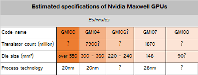
nvidia_maxwell_estimated_specs
Still, what we do know is that a chip featuring 7.9 billion of transistors should be made using 20nm process technology in order to hit the same price-points as the GK104 did. It is also pretty logical to expect the flagship GM100/GM110 chip to be made using 20nm fabrication process. At the same time, it is possible that Nvidia could make GM106 chip using 28nm fabrication process to completely replace all the GK106-based solutions as well as graphics boards powered by cut-down versions of the GK104.
Summing up
All-in-all, while it is possible that the GM104 (and GeForce GTX 880) will indeed be made using 20nm fabrication process, consist of 7.9 billion of transistors and contain 3200 stream processors (thus beating the GeForce GTX Titan Black in many applications), chances that it will be released this summer are pretty thin, unless there is a major development with yields at Taiwan Semiconductor Manufacturing Co.
Nvidia and TSMC did not comment on the news-story. Link